I recently completed the design and implementation of my Final Year Project. However, during the simulation phase near the end, I realized that the Cyclone V SX SoC Development Kit wasn’t the best match for this type of project. As I said I would in my previous post, I discussed this with my supervisor, and fortunately, I got my hands on not only the DE1 board but also the DE2.
I want to dedicate this post not only to testing and simulating my FYP design, but also to sharing my approach to using FPGA development boards and how I deal with them.
I have experience with the DE1 board from my Digital Computer Design course labs. It’s a solid and reliable board, easy to work with. But after giving it some thought, I realized that choosing the DE1 over the DE2 would be a big mistake. The DE2 board offers more advanced features and higher performance, like an improved version of the DE1, even down to its layout. That’s why I’ll go with it.
Knowing The Board
Starting with the user manual is a smart move to know the board. I usually just skim through the important parts instead of reading it all in detail. The most important aspects for us are understanding the layout, components, and pin assignments of the board.
Pin assignments determine which physical pins on the FPGA are connected to specific components, so that we can map our logical design to physical hardware. For example, in DE2 board, we have 18 switches. By referring to the pin table, we can find their pin assignments. Now that everything makes sense, we’re good to go.
Burning VHDL
Let’s start with a simple VHDL design to burn onto the board and then try simulating it. I want to program the board so that different two-bit inputs from switches SW0 and SW1 will display different characters on one of the seven-segment displays. For example, when the input is ‘00’, it will display ‘S’, for ‘01’ it will display ‘A’, for ‘10’ it will display ‘E’, and for ‘11’ it will display ‘B’.
library IEEE;
use IEEE.std_logic_1164.all;

entity SevenSegmentDisplay is
	port(
			-- Input
			charSelect : in std_logic_vector(1 downto 0); -- Character selection

			-- Output
			segDisplay :  out std_logic_vector(6 downto 0) -- 7-Segment display
		);
end SevenSegmentDisplay;

architecture Behavioral of SevenSegmentDisplay is
begin
	process(charSelect)
	begin
		case charSelect is
			when "00" => segDisplay <= "0010010"; -- Displays 'S'
			when "01" => segDisplay <= "0001000"; -- Displays 'A'
			when "10" => segDisplay <= "0000110"; -- Displays 'E'
			when "11" => segDisplay <= "0000000"; -- Displays 'B'
			when others => segDisplay <= "1111111"; -- All segments off
		end case;
	end process;
end Behavioral;
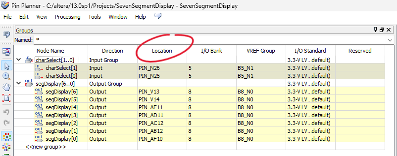
Using Intel Quartus Web Edition this time is a good choice. Following the user manual, it’s important to select the device when creating a new project. Then, we assign the logical ports to physical pins on the board using the pin planner, following the pin table as before.
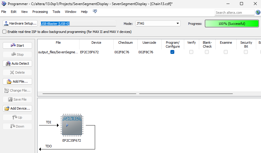
Next, we move to the Programmer tool, where we carry out the process of burning the VHDL code onto the FPGA on the board, along with all the mapped pins.
Now we simulate!
Before returning to our MIPS ALU, let’s add a twist. I want to make use of four consecutive seven-segment displays, with each segment being controlled by two switches, totaling 8 switches for all displays.
library IEEE;
use IEEE.std_logic_1164.all;

entity MultiSegmentDisplay is
    Port(
	    	-- Input
	        switches : in std_logic_vector(7 downto 0); -- 8 switches

	        -- Output
	        seg_display : out std_logic_vector(27 downto 0) -- 4 seven-segment displays, each 7 bits
    	);
end MultiSegmentDisplay;

architecture Behavioral of MultiSegmentDisplay is
begin
    process(switches)
    begin
        -- Display 1, controlled by switches(1 downto 0)
        case switches(1 downto 0) is
            when "00" => seg_display(6 downto 0) <= "0010010"; -- 'S'
            when "01" => seg_display(6 downto 0) <= "0001000"; -- 'A'
            when "10" => seg_display(6 downto 0) <= "0000110"; -- 'E'
            when "11" => seg_display(6 downto 0) <= "0000000"; -- 'B'
            when others => seg_display(6 downto 0) <= "1111111"; -- All segments off
        end case;

        -- Display 2, controlled by switches(3 downto 2)
        case switches(3 downto 2) is
            when "00" => seg_display(13 downto 7) <= "0010010";
            when "01" => seg_display(13 downto 7) <= "0001000";
            when "10" => seg_display(13 downto 7) <= "0000110";
            when "11" => seg_display(13 downto 7) <= "0000000";
            when others => seg_display(13 downto 7) <= "1111111";
        end case;

        -- Display 3, controlled by switches(5 downto 4)
        case switches(5 downto 4) is
            when "00" => seg_display(20 downto 14) <= "0010010";
            when "01" => seg_display(20 downto 14) <= "0001000";
            when "10" => seg_display(20 downto 14) <= "0000110";
            when "11" => seg_display(20 downto 14) <= "0000000";
            when others => seg_display(20 downto 14) <= "1111111";
        end case;

        -- Display 4, controlled by switches(7 downto 6)
        case switches(7 downto 6) is
            when "00" => seg_display(27 downto 21) <= "0010010";
            when "01" => seg_display(27 downto 21) <= "0001000";
            when "10" => seg_display(27 downto 21) <= "0000110";
            when "11" => seg_display(27 downto 21) <= "0000000";
            when others => seg_display(27 downto 21) <= "1111111";
        end case;
    end process;
end Behavioral;
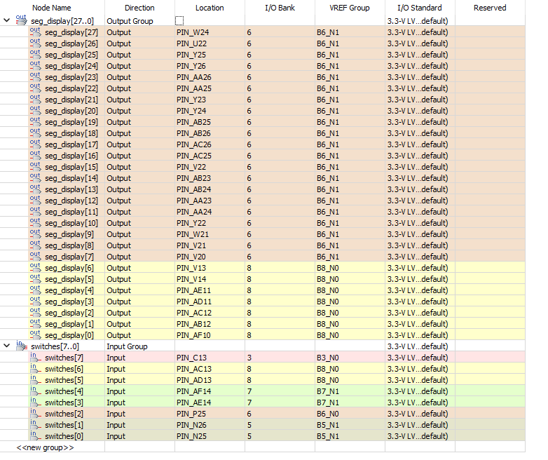
Back To 32-Bit MIPS ALU
In a single-cycle MIPS CPU design, like mine, every instruction is designed to execute in a single clock cycle. This means that all the stages of instruction execution—fetch, decode, execute, memory access, and write-back—occur within a single clock cycle. The cycle’s length is based on the time it takes for the slowest instruction. This is usually determined by the longest path an instruction takes, often the load word (lw) instruction.
While this single-cycle approach simplifies the control logic and makes it easier to understand and implement, it usually needs a longer clock period to handle the slowest instruction because all operations must finish within one cycle. This can restrict the CPU’s overall clock speed. In contrast, multi-cycle architectures spread different stages of instruction execution over multiple cycles, potentially enabling a higher clock speed but demanding more complex control logic.
Let me break down everything that should happen in a single cycle:
-
Instruction Fetch: The instruction is fetched from the Instruction Memory, where our test program is.
-
Instruction Decode: The fetched instruction is decoded to understand what operation is to be performed and which registers are involved.
-
Exectue: The operatoin specified by the instruction is executed, which might invovle arithmetic or logical operations in the ALU, address calculation for memory operations, etc.
-
Memory Access (if needed): Data is read from or written to the memory.
-
Write-back: The result of the execution is written back to a register if required by the instruction.
Since I didn’t write a test bench for the top level module I implemented in the design, let’s write one now.
library IEEE;
use IEEE.std_logic_1164.all;

entity TopLevel_tb is
    -- No ports required
end TopLevel_tb;

architecture behavior of TopLevel_tb is
    component TopLevel
        GENERIC (n : integer := 32);
        port(
            CLK, reset_neg : in std_logic
        );
    end component;

    signal CLK, reset_neg : std_logic := '0';

begin
    -- Instantiate the Unit Under Test (UUT)
    uut: TopLevel
        generic map (n => 32)
        port map (
            CLK => CLK,
            reset_neg => reset_neg
        );

    -- Clock generation
    clocking: process
    begin
        for i in 1 to 20 loop  -- Each cycle is 20 ns, 20*10 ns = 200 ns for 10 instructions
            CLK <= not CLK;  -- Toggle clock
            wait for 10 ns;  -- Half period of 20 ns cycle
        end loop;
        wait;  -- Stop after the last cycle
    end process;

    initial_setup: process
    begin
        reset_neg <= '0';  -- Assert
        wait for 20 ns;    -- Hold reset for initialization
        reset_neg <= '1';  -- Deassert
        wait;              -- Continue until simulation stops after 200 ns
    end process;

end behavior;
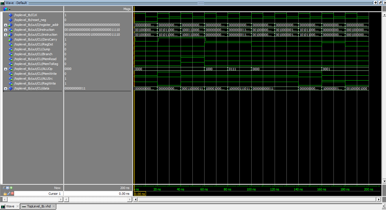
This test bench simulates the operation of the single-cycle MIPS CPU, focusing on the sequential execution of 10 instructions across 10 full clock cycles, totaling 200ns. It initializes the clock and active-low reset signals, toggling the clock every 10ns to maintain a 50MHz frequency, thereby establishing a 20ns clock period. The reset is initially asserted and then deasserted to ensure the processor starts from a known state.
Note
I screenshotted the waveform from Intel ModelSim software, as I couldn’t find a better way to export it in higher quality. For better viewing, open it in a new tap. Feedback from experienced users on waveform exporting is welcome.
Let’s take the first full cycle of our execution, which is according to our test program inside our Instruction Memory is an I-type instruction addi $R1, $R0, 30.
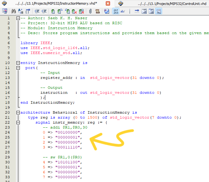
As I detailed in my design post, each MIPS instruction spans 32 bits, which is equivalent to 4 bytes. To accommodate this in the Instruction Memory, I allocated four consecutive memory addresses for each individual instruction. Similarly, the Assembler operates by encoding each instruction into 4 bytes to align with our design. It’s important to note that if an instruction begins at address 0, it will occupy the bytes at addresses 0, 1, 2, and 3. Hence, to move to the next instruction, we increment the program counter by 4. For further details, refer to the Memory Instruction section in my previous blog post.
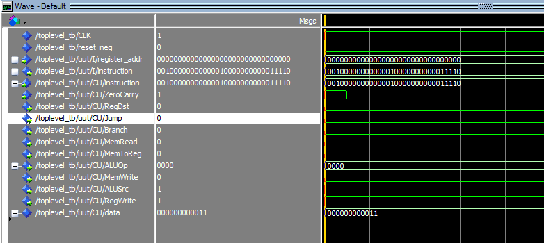
Now we can clearly see that our complete 32-bit instruction is the concatenation of the 4 bytes occupying the first 4 addresses: 0, 1, 2, and 3, resulting in the full instruction 00100000000000010000000000011110.
According to the way I designed the Control Unit, which generates control signals for various components within the processor based on our input instruction (addi in this case), we should expect an 11-bit data signal to set the control signals. In our case, the data signal is 000000000011, which perfectly aligns with our implementation.
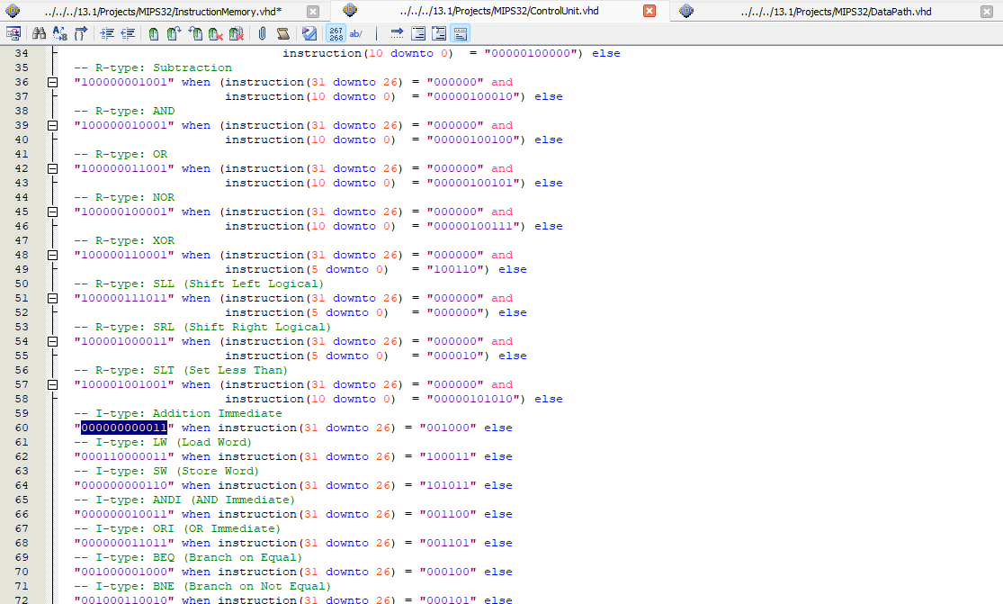
Returning to our primary focus, the ALU, we observe that the ALUOp, indicating the ALU operation to be performed, is set to 0000. This precisely matches our design, where 0000 signifies addition operations.
Moving to the next instruction sw $R1,0($R0).
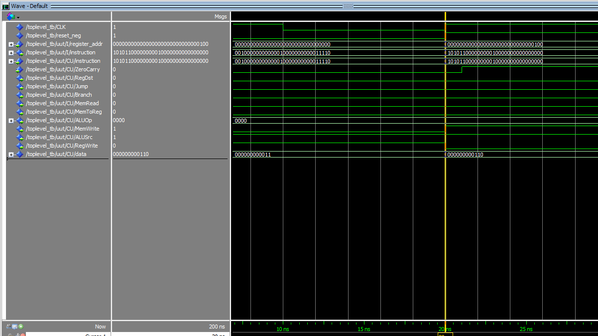
The full instruction, 10101100000000010000000000000000, perfectly aligns with our layout in the Instruction Memory. Additionally, the data signal, 000000000110, matches the control signal settings in the Control Unit. Regarding the ALUOp, it remains at 0000 because this instruction is a Memory write (store word), not an ALU operation. However, if you review the waveform, you’ll notice that the ALUOp changes multiple times, indicating that we encountered 5 ALU operations in our test program.
With our DE2 board, we can supply a 50MHz clock, achieving the same results.
Conclusion
This marks the conclusion of one of the most enjoyable and challenging projects I’ve worked on. Undoubtedly, in the days to come, I’ll encounter numerous bugs and mistakes, as is typical with any project. I’ll do my best to update these blogs regularly, but for now, that’s all.
Source Code
You can find all the code here.
Last Edited: Jan 20, 2024