I’ve recently started my Final Year Project with a focus on designing a 32-bit MIPS Arithmetic Logic Unit (ALU) based on RISC, and one thing became clear: the basics are absolutely crucial. Things like logic, boolean algebra, and digital design form the foundation for everything in this field. Even in the simple CHIP-8 Emulator I built last time, I found myself deep in low-level bit manipulation. This included working with binary, hex, logical operators, bitmasking, bit shifting, and more. It’s for this reason that I’m putting together this blog post, which will serve as a primer or refresher for all the specialized topics I’ll dive into in future blog posts. Additionally, I plan to document my ongoing journey in designing the ALU. I hope this documentation can be a valuable resource for others keen on learning about digital design and computer architecture.
- Low-level Bit Manipulation
- Logic Gates
- Boolean Algebra
- Computer Abstraction Hierarchy
- Instruction Set Architecture (ISA)
- RISC vs CISC: ISA wars
- MIPS
- Conclusion
Low-level Bit Manipulation
I’m beginning with this topic because it’s a daily essential and a critical aspect of every project, particularly in our earlier CHIP-8 emulator.
Binary
Bits represent one of two values, 0 or 1, and together they form binary numbers. Computers operate on numbers in the form of binary, which is base-2, chosen for hardware simplicity. Binary’s base-2 nature aligns perfectly with the electronic components inside computers, where it’s easier to distinguish between two voltage levels (high and low) than it is to differentiate between multiple levels (computers use switches, such as transistors, that can be either on or off).
Note:
The transistor will go down as one of the greatest inventions in modern history. To put it simply, a transistor is a tiny electronic device to control the flow of electricity. But a transistor is more than that. It has two key abilities: the first is to amplify an electric signal, and the other is to switch on or off (1 or 0), letting current through or blocking it as necessary. Transistors are in practically all modern electronics these days. Since its invention, it has made the computer revolution possible by making it cheaper and cheaper to pack more transistors onto a computer chip every year (this is known as Moore’s Law, which Intel founder Gordon Moore defined. He said that every year manufacturing would get so good that double the number of transistors would be able to fit on a chip for the same price). A simple logic gate comprises about twenty transistors, compared to an advanced computer chip in a modern computer, which can include as many as a billion transistors.
Any number can be represented in binary. Binary is all about powers of 2. There is a pattern to binary that helps with understanding it. Here is the sequence from 0 to 15:
|3|2|1|0|
---------
|0|0|0|0| => 0
|0|0|0|1| => 1
|0|0|1|0| => 2
|0|0|1|1| => 3
|0|1|0|0| => 4
|0|1|0|1| => 5
|0|1|1|0| => 6
|0|1|1|1| => 7
|1|0|0|0| => 8
|1|0|0|1| => 9
|1|0|1|0| => 10
|1|0|1|1| => 11
|1|1|0|0| => 12
|1|1|0|1| => 13
|1|1|1|0| => 14
|1|1|1|1| => 15Decimal, our familiar base-10 system, is where numbers count up from 0 to 9 before shifting over to the left as they grow larger. For instance, 9 becomes 10, 19 becomes 20, and this pattern continues. Binary, a base-2 system, works similarly but with just 0 and 1. So, it goes from 0b0001 to 0b0010, 0b0011 to 0b0100, and so on. It’s a simpler but equally systematic way of counting and representing numbers in the digital world.
In base-10, each place represents a power of 10, allowing us to express numbers of different magnitudes. For example, in 528, the ‘ones’ place has 8, the ’tens’ place holds 2 and the ‘hundreds’ place contains 5. We calculate the number by multiplying each place’s value by its respective power of 10 and summing them: (5 * 10^2) + (2 * 10^1) + (8 * 10^0) = 528.
Again, binary works similarly, but with powers of 2. In binary, the ‘ones’ place is 2^0 (1), the ’twos’ place is 2^1 (2), and so on. For instance, in 0b101, the ‘ones’ place is 1, the ’twos’ place is 0, and the ‘fours’ place is 1. By multiplying each digit by its corresponding power of 2 and adding them, we find the binary number’s value: (1 * 2^2) + (0 * 2^1) + (1 * 2^0) = 5.
Bit 0 is called the Least Significant Bit (LSB), residing in the ‘ones’ place (2^0), holds the least contribution to the final value of a binary number. On the other hand, we have Bit 3, which is called the Most Significant Bit (MSB), positioned in the ’eights’ place (2^3), holds the most contribution to the final value of a binary number.
Hexadecimal
Coping with binary can be challenging for humans when dealing with more than four bits. This is where hexadecimal, or ‘hex’ for short, comes to the rescue. Hexadecimal is a base-16 system, offering a compromise between binary and our familiar base-10. While base-2 has only 0 and 1, and base-10 goes from 0 through 9, hexadecimal extends further, including not only 0 through 9 but also A through F. Counting in hexadecimal follows the same principles as base-2 and base-10, but with the unique twist of adding letters.
- A = 10
- B = 11
- C = 12
- D = 13
- E = 14
- F = 15.
Let’s take this hexadecimal number 0xCAFE :) as an example:
0xCAFE = (C * 16^3) + (A * 16^2) + (F * 16^1) + (E * 16^0) = 51966
In binary, this would be expressed as 0b1100101011111110.
Note:
Sometimes you might come across numbers prefixed with ‘0x’ or ‘0b’. These prefixes are essential for indicating the number’s base. 0x indicating hexadecimal and 0b signifying binary. C++ recognizes hexadecimal numbers when they start with ‘0x’ and binary numbers when they start with ‘0b’.
Bits and Bytes
In the binary system, a single digit is known as a bit, which can be either ‘ON’ (1) or ‘OFF’ (0). A byte consists of eight bits, allowing it to reach a maximum value of 255 (2^8 - 1, since we start from the zero). In hexadecimal, this is represented as 0xFF.
Commonly used multiples include 1 byte (0xFF), 2 bytes (0xFFFF), 4 bytes (0xFFFFFFFF), and 8 bytes (0xFFFFFFFFFFFFFFFF).
Logical Operators
Besides understanding how to read binary and hex, it’s important to know how to manipulate them with some common operations: AND, OR, NOT, and XOR.
They are explained better in table form:
|       AND       |       OR         |    NOT    |       XOR       |
|-----|-----|-----|-----|-----|------|-----|-----|-----|-----|-----|
|  0  |  0  |  0  |  0  |  0  |  0   |  0  |  1	 |  0  |  0  |  0  |
|  0  |  1  |  0  |  0  |  1  |  1   |  1  |  0  |  0  |  1  |  1  |
|  1  |  0  |  0  |  1  |  0  |  1   |  -  |  -  |  1  |  0  |  1  |
|  1  |  1  |  1  |  1  |  1  |  1   |  -  |  -  |  1  |  1  |  0  |
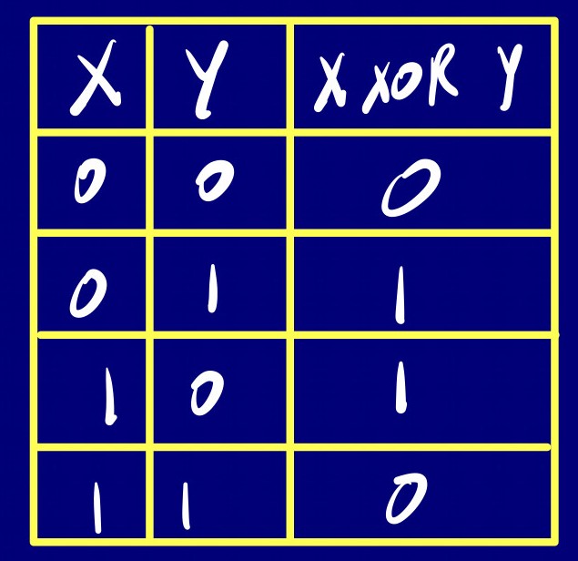
AND spits true if both bits are true, while OR is true if either bit is true. NOT toggles the bit, and XOR is true if only one bit is true.
In C++, AND is represented by the symbol &, OR by |, NOT by ~, and XOR by ^. These logical operators also have corresponding gates in digital circuit design, which we’ll discuss later.
Bitmasking
Bitmasking is like using a special pattern (the “mask”) to pick out or change specific parts of a binary number. By performing bitwise operations like AND, OR, or XOR between the bitmask and the target number, you can control or extract certain bits while leaving others unchanged.
=> AND is good for clearing bits:
Let’s say we have the binary number 0b1101, and we want to clear Bit 0 (1), which means making it 0. To do this, we can use AND. Here’s what happens:
- Create a bitmask with all bits set to 1 except for Bit 0, which should be set to 0. The bitmask is 0b1110
- Perform a bitwise AND operation between the original number (0b1101) and the bitmask (0b1110).
	0b1101
AND
	0b1110
--------------
	0b1100 (Bit 0 cleared: before it was 1, now it's 0)
=> OR is good for setting bits:
Taking our previous number 0b1101 as our target number, and we want to set Bit 1 (0), which means making it 1, we can OR it with 0b0010 mask.
	0b1101
OR
	0b0010
--------------
	0b1111
=> XOR is good for many things:
One common application for XOR is to clear a register by XORing it with itself.
Let’s say that I want to clear our target number 0b1101 to zeros, we can use XOR.
	0b1101
XOR
	0b1101
--------------
	0b0000
Bit Shifting
Bit shifting is a process of moving individual bits left («) or right (») in a binary number. Left shifting multiplies the number by 2 for each shift, while right shifting divides it by 2.
Left Shift (<<):

0b1010 (10) <- 0b0101 (5)

Right Shift (>>):

0b1010 (10) -> 0b0101 (5)
Logic Gates
Logic gates are digital circuits that take one or more binary inputs and produce a binary output. You can check out the basis of logic with Boolean Algebra .
Think of a logic gate as an elementary standalone chip designed to deliver a functionality.
Elementary
There are three basic logic gates that we are going to go over, just keep in mind that no matter how many inputs, the action of any gate is exactly the same. Each of these gates has a related truth table and logic symbol.
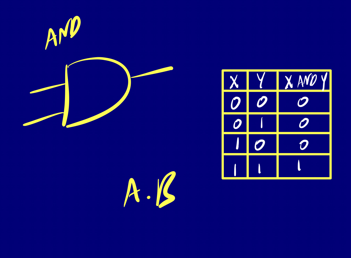
=====
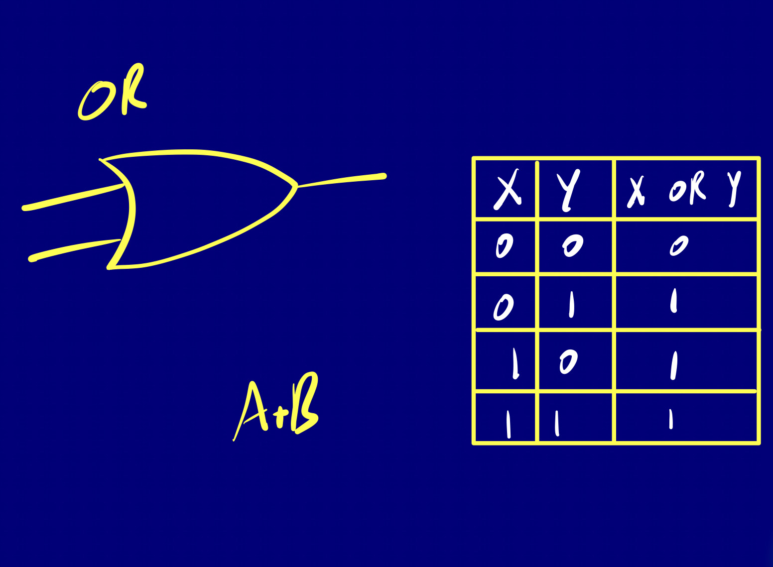
=====
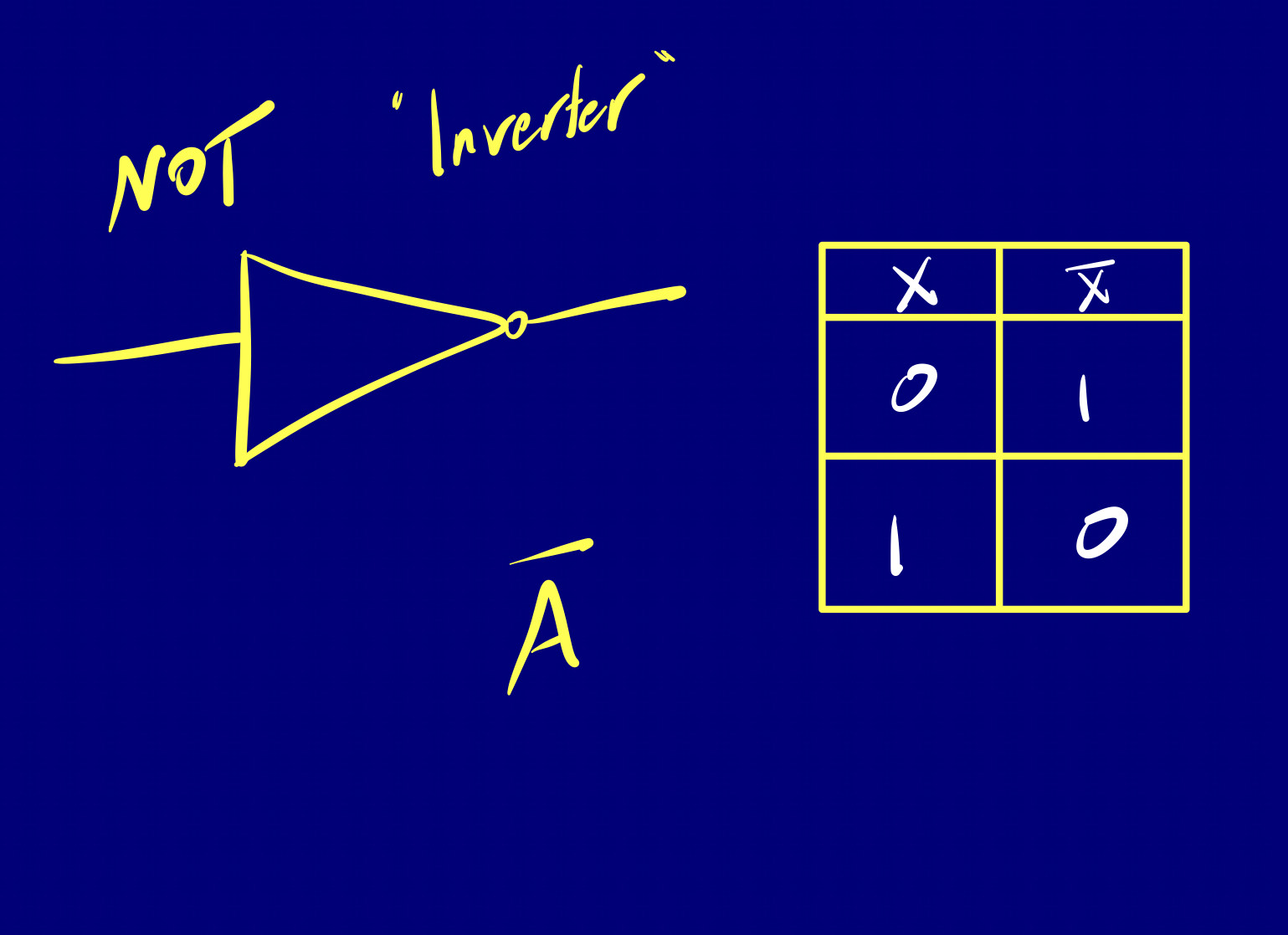
These three logic gates form the building blocks of all digital circuits. Whether it’s a simple adder (composite logic gate) or a complex processor, they’re all composed of combinations of these basic gates.
Composite
Composite gates are created by combining elementary gates in various ways to perform more complex logical functions. For example, a Multiplexer (MUX) or a Flip-Flop is a composite gate because they are constructed using combinations of elementary gates. Even NAND, NOR, and XOR are considered simple composite gates.
Looking into NAND, which is simply the negation of AND. To make a NAND gate where the output is 0 if and only if both inputs are 1, we can use an AND gate followed by a NOT gate.
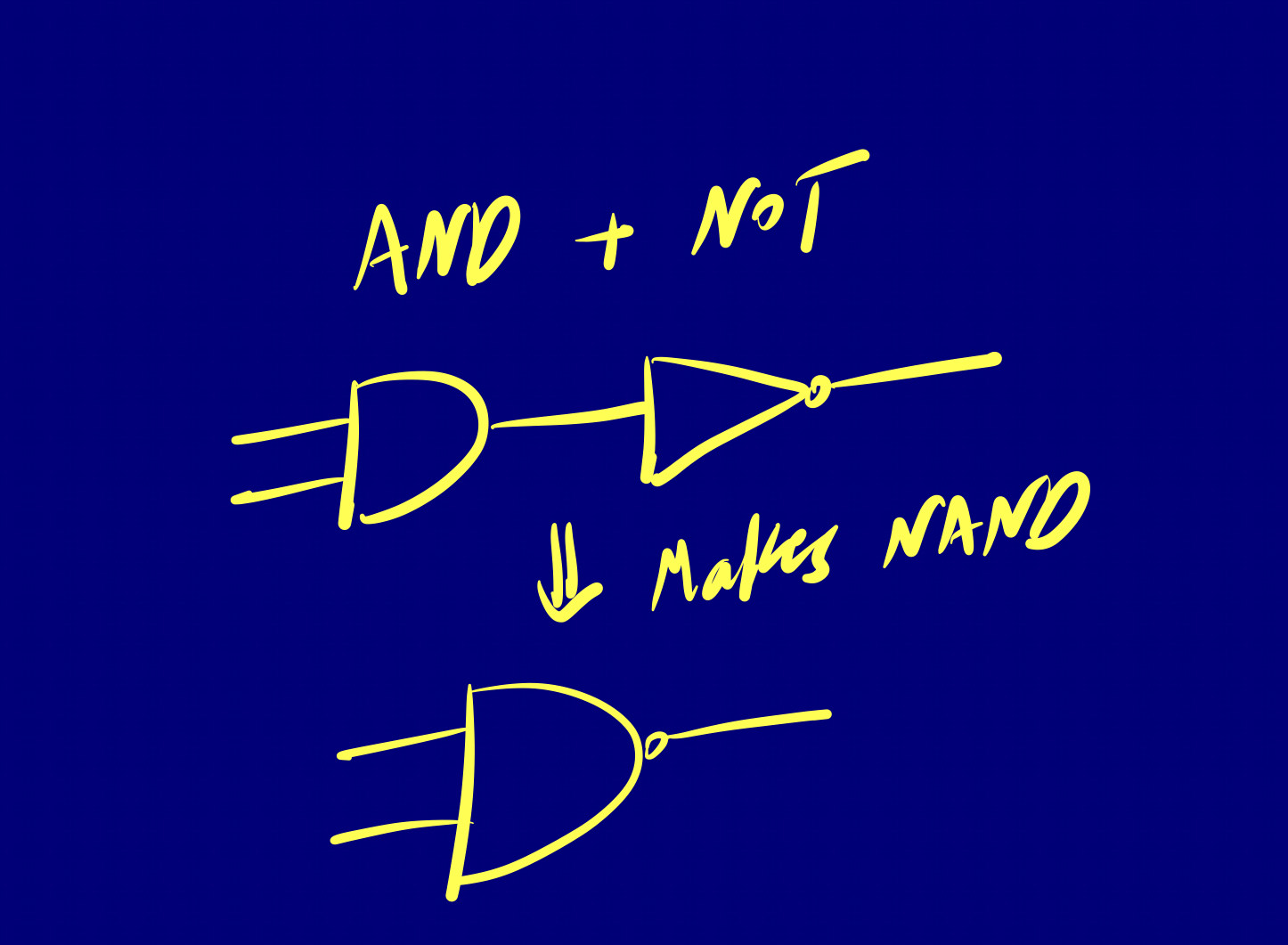
There’s also NOR, which is the negation of OR.
=====
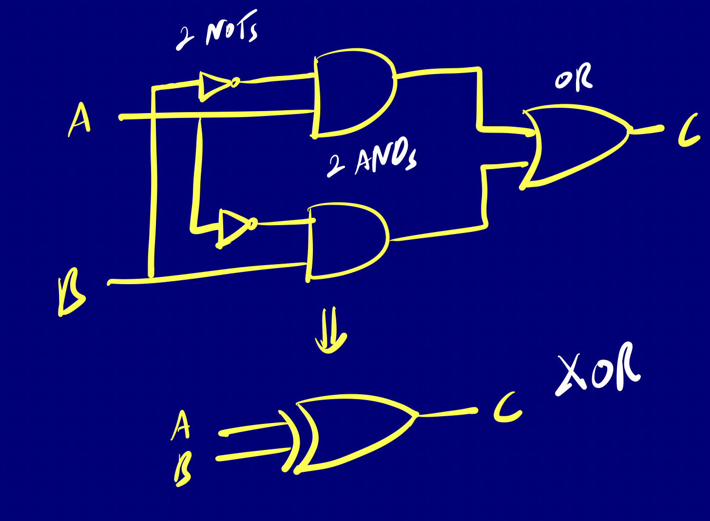
A more interesting example is the XOR gate we discussed earlier in the Logical Operators, and used extensively in the CHIP-8 emulator. Its output is 1 if the inputs are not the same. We can see how this works by looking at its implementation. It is built with 2 NOT’s, 2 AND’s and an OR gate.
Boolean Algebra
Earlier, I introduced bits and the binary number system from an arithmetic viewpoint. But here’s the twist – bits aren’t just numbers; they embody logical qualities, toggling between on/off, true/false, or present/not present. This abstract, logical understanding forms the backbone of boolean algebra.
Boolean algebra is a set of rules to play with true and false statements or 1s and 0s. You use these rules to build logical conditions and make decisions in computer programming and digital systems.
For example, I can define a boolean function of three inputs
f(x,y,z) = (x AND y) OR (NOT(x) AND z)The really nice thing about boolean values is the fact that there are only a finite number of possible inputs, and we can easily list them, like we did before.
|  x   	 y     z  |  f	|
|-----|-----|-----|-----|
|  0  |  0  |  0  |  0	|
|  0  |  0  |  1  |  1	|
|  0  |  1  |  0  |  0	|
|  0  |  1  |  1  |  1	|
|  1  |  0  |  0  |  0	|
|  1  |  0  |  1  |  0	|
|  1  |  1  |  0  |  1	|
|  1  |  1  |  1  |  1	|
Note:
Notice that we have parentheses in the boolean function, which indicate priority.
The table of values that we have, gives the same information as the previous boolean function formula. So there are two ways in which we described the boolean function, the first was the formula, the second was the truth table.
The last thing I want to focus on is boolean identities, which define how logical expressions can be manipulated and simplified. They play a crucial role in constructing, analyzing, and optimizing logical conditions, so understanding them empowers us to streamline complex boolean expressions, making them more manageable.
1- Commutative Law:
This law applies to both the AND and OR operations. For AND, it states that A AND B is equivalent to B AND A. Similarly, for OR, it states that A OR B is the same as B OR A.
Symbolically:
A AND B = B AND A
A OR B = B OR A
2- Associative Law:
The Associative Law is also applicable to both AND and OR operations. For AND, it states that (A AND B) AND C is the same as A AND (B AND C). Similarly, for OR, it states that (A OR B) OR C is equivalent to A OR (B OR C).
Symbolically:
(A AND B) AND C = A AND (B AND C)
(A OR B) OR C = A OR (B OR C)
3- Distributive Law:
The Distributive Law connects AND and OR operations. For example, A AND (B OR C) is equivalent to (A AND B) OR (A AND C).
Symbolically:
A AND (B OR C) = (A AND B) OR (A AND C)4- De Morgan's Laws:
De Morgan’s Laws describe the relationship between AND, OR, and NOT operations. For AND, it states that NOT (A AND B) is the same as (NOT A) OR (NOT B). Similarly, for OR, it states that NOT (A OR B) is equivalent to (NOT A) AND (NOT B).
Symbolically:
NOT (A AND B) = (NOT A) OR (NOT B)
NOT (A OR B) = (NOT A) AND (NOT B)
By applying these identities, we can simplify a boolean expression or just bring it into a different format.
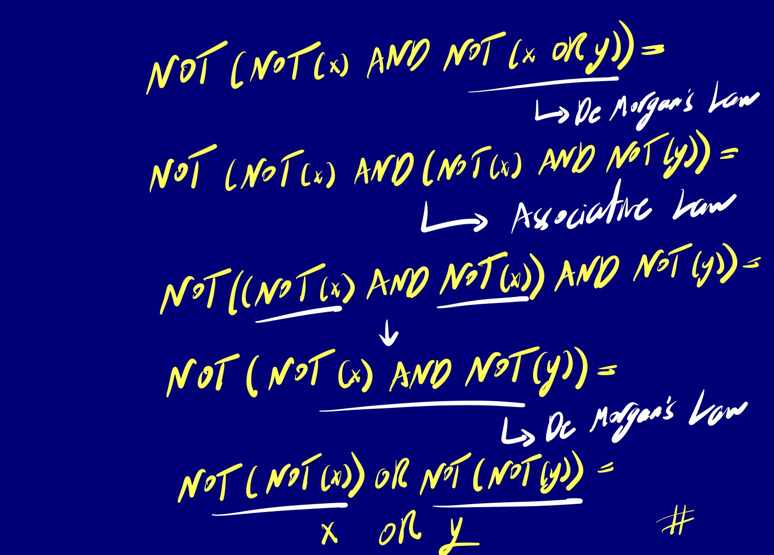
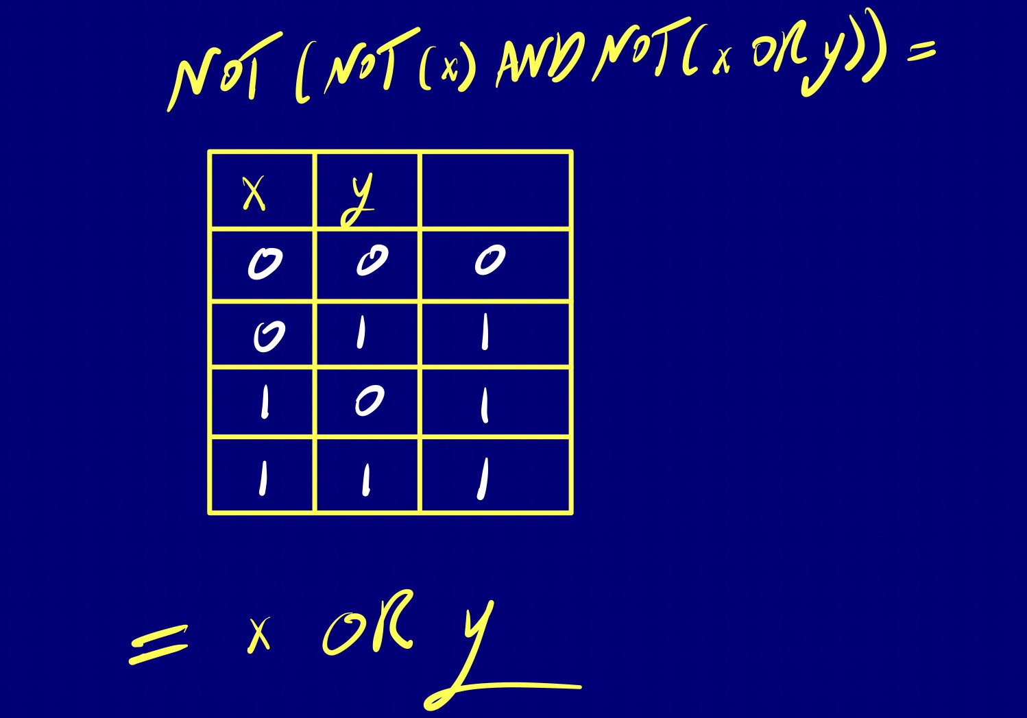
There’s also another way to get the same equivalence without going through these algebraic manipulations, simply by building a truth table.
For a more detailed exploration of Boolean Algebra, check out this .
Computer Abstraction Hierarchy
The way a computer works on the inside has levels of abstraction. The computer abstraction hierarchy is a conceptual framework that organizes the various levels of abstraction within a computer system, helping us understand its complexity by breaking it down into manageable layers. This hierarchy consists of three main domains: the Software Domain, Digital Domain, and Analog Domain.
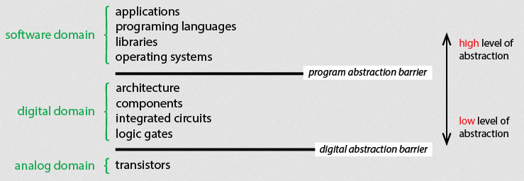
The representation of this hierarchy can vary, so these levels aren’t always the same. The crucial abstraction levels to keep in mind include software, digital computer hardware, and the underlying analog circuit components.
For instance, look at this other representation.
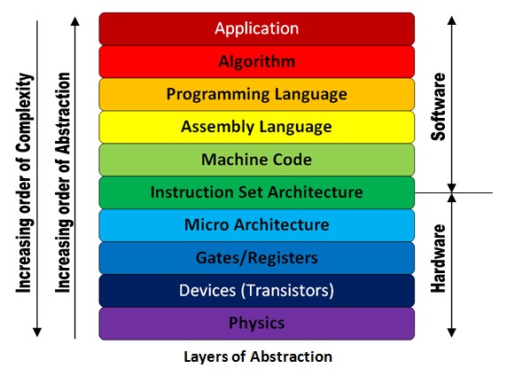
If this is your first encounter with the computer abstraction hierarchy, check this for a helpful introduction and more details.
Instruction Set Architecture (ISA)
To put it in the simplest way, ISA defines the interface which hardware presents to software. A compiler translates high-level source code (e.g., C++) to the ISA for a target processor then the processor directly executes ISA instructions.
Examples of ISAs include MIPS, ARM (popular on mobile devices), and x86 (popular on desktops and laptops; known to cause sadness among programmers and hardware developers).
It’s good to mention that we have three basic types of instructions:
- Arithmetic/bitwise logic (e.g., addition, or left-shift).
- Data transfers to/from/between registers and memory.
-
Control flow
- Unconditionally jump to an address in memory.
- Jump to an address if a register has a value of 0.
- Invoke a function.
- Return from a function.
RISC vs CISC: ISA wars
Starting with CISC (Complex Instruction Set Computer), the ISA has a large number of complex instructions, what I mean by “complex” here is that a single instruction can do many things. For instance, a single hardware instruction has to do a branch, a memory read, a memory write, and maybe two register increments or decrements, so that’s a lot!
CISC instruction are often variable-size (can be of different sizes) to minimize RAM usage. CISC instructions make life easier for compiler writers, but much more difficult for hardware designers—complex instructions are hard to implement and make fast. x86 is the classic CISC ISA.
On the other hand, in RISC (Reduced Instruction Set Computer), the ISA has a smaller number of simple instructions. RISC hardware only needs to do a few, simple things well—thus, RISC ISAs make it easier to design fast, power-efficient hardware. RISC ISAs usually have fixed-sized instructions and a load/store architecture. MIPS and ARM (Advanced RISC Machine) are classic RISC ISAs.
Consider this example of multiplying two values:
For CISC, the instruction ‘MULT’ is specifically designed to handle the multiplication of two values. It’s a single, complex instruction that takes care of the entire task.
MULT A,BIn contrast, RISC divides the ‘MULT’ operation into three separate commands, each performing a specific task.
LOAD R1, A     ; Load value A into register R1
LOAD R2, B     ; Load value B into register R2
PROD R1, R2    ; Multiply values in R1 and R2, store result in R1
STORE R3, R1    ; Store the result back into memory or another register
This breakdown into smaller, simpler instructions is characteristic of the RISC philosophy, where each instruction performs a basic operation, making it easier to design efficient hardware. It also allows for more flexibility in programming, as each step can be customized if needed.
In short, CISC is like having a lot of fancy tools in one, and RISC is like having just the right tools for the job. People use CISC for big computers, and RISC is popular in smaller gadgets.
For more on CISC and RISC, check this cool video .
MIPS
MIPS (Microprocessor without Interlocked Pipeline Stages) is a RISC architecture commonly used in processors. In simple terms, MIPS keeps things streamlined by using a smaller set of instructions that execute in a single clock cycle. This simplicity makes it a solid choice for educational purposes and projects. The basic MIPS structure includes components like registers, an ALU, and a control unit.
The “without interlocked pipeline stages” part emphasizes a key feature of the MIPS architecture.
In a pipelined processor, instructions move through a series of stages (like fetch, decode, execute) in a pipeline fashion, where each stage performs a specific part of the instruction execution. Interlocked pipeline stages mean that the stages are closely connected or dependent on each other, and the progress of one stage may affect the progress of others.
MIPS, being a RISC architecture, aims for simplicity and efficiency. The absence of interlocked pipeline stages means that each stage of the pipeline operates independently and doesn’t depend heavily on the completion of the previous stage.
The key concepts of MIPS architecture are:
- Five-stage execution pipeline: fetch, decode, execute, memory-access, write-result.
- Regular instruction set, all instructions are 32-bit.
- Three-operand arithmetical and logical instructions.
- 32 general-purpose registers of 32-bits each.
- No complex instructions (like stack management, etc.).
- Only the load and store instruction access memory.
Three basic instruction formats
MIPS defines three basic instruction formats:
R-type
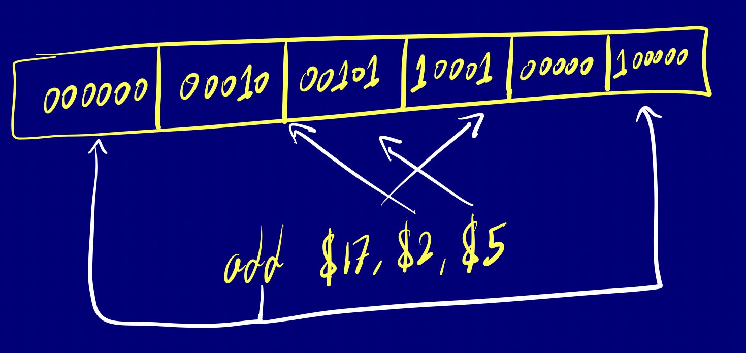
R-type instructions are primarily used for arithmetic and logical operations. They involve three registers (source1, source2, and destination) and perform an operation like addition, subtraction, AND, OR, etc.
op $dest, $src1, $src2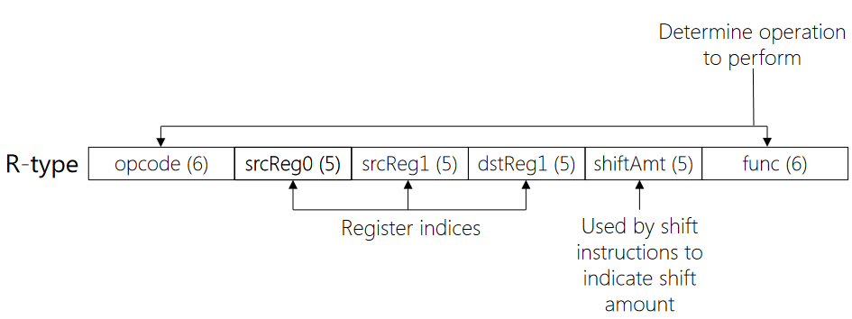
I-type
I-type instructions handle immediate values (constants) in addition to registers. These are often used for data transfer and immediate arithmetic/logical operations.
op $dest, $src1, immediate
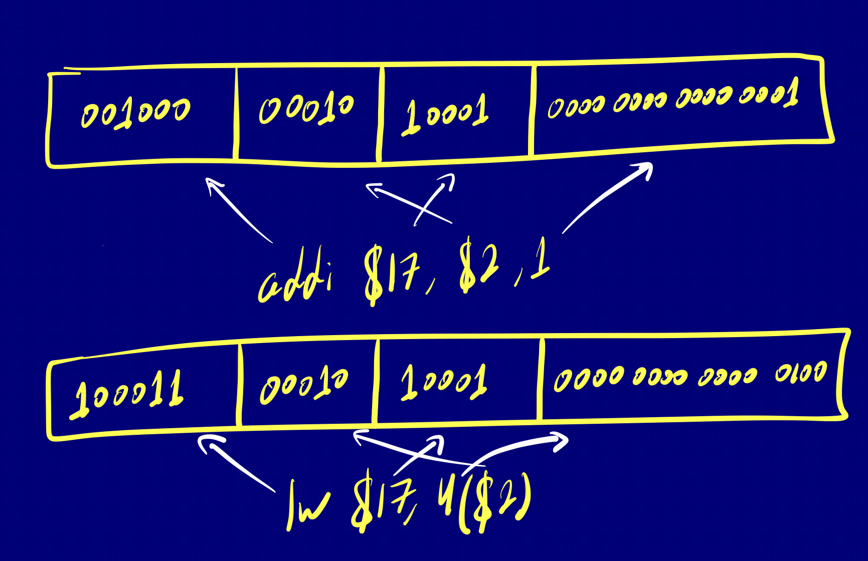
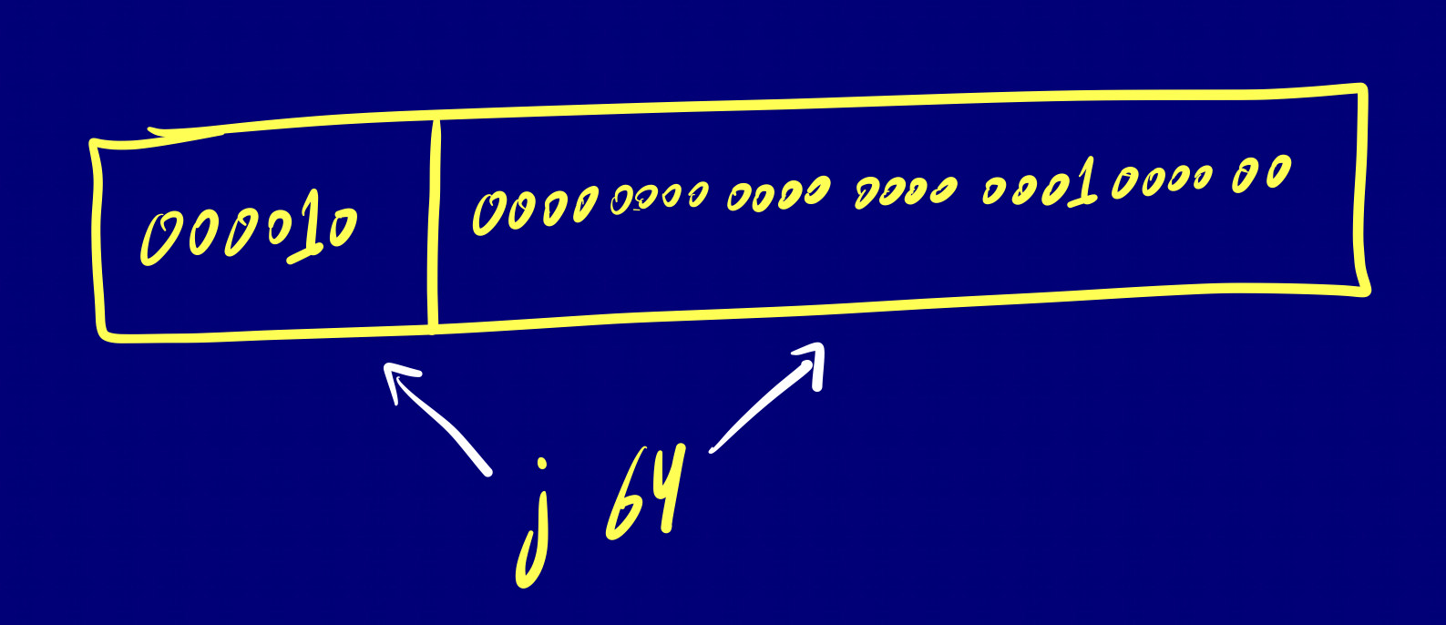
J-type
J-type instructions are primarily used for jump and branch operations. They involve a target address for the jump.
j target_address
Load/Store Architecture
Except for load and store instructions, all other instructions require register or constant (“immediate”) operands. ‘Load’ reads a value from a memory address into a register, and ‘Store’ writes a value from a register into a memory location.
So, to manipulate memory values, a MIPS program must:
- Load the memory values into registers.
- Use register-manipulating instructions on the values.
- Store those values in memory.
Note:
Load/store architectures are easier to implement in hardware. You don’t have to worry about how each instruction will interact with complicated memory hardware!
Building A Processor To Execute MIPS Instructions
I read once a great example that simplifies the process of building a processor to execute MIPS instructions, and it’s akin to designing a car manufacturing factory. Let’s dive into this analogy:
Factory Design #1 - The Single, Complex Robot: Imagine building a car assembly line where constructing a car involves three sequential tasks. These tasks cannot overlap, and each takes the same amount of time. Now, picture a single, sophisticated robot designed to perform all of these tasks. In this scenario, the factory completes one car every three time units (t=0, t=1, t=2). The robot progresses through each task in sequence.
Factory Design #2 - The Three Simple Robots: On the other hand, consider an alternative approach. Instead of one complex robot, we design three simpler robots, each dedicated to performing one specific task. These robots can operate in parallel, simultaneously working on different cars. As the factory ramps up, it achieves the remarkable feat of producing one car every time unit. The tasks are distributed among the specialized robots, and cars are efficiently produced, one after another, in quick succession.
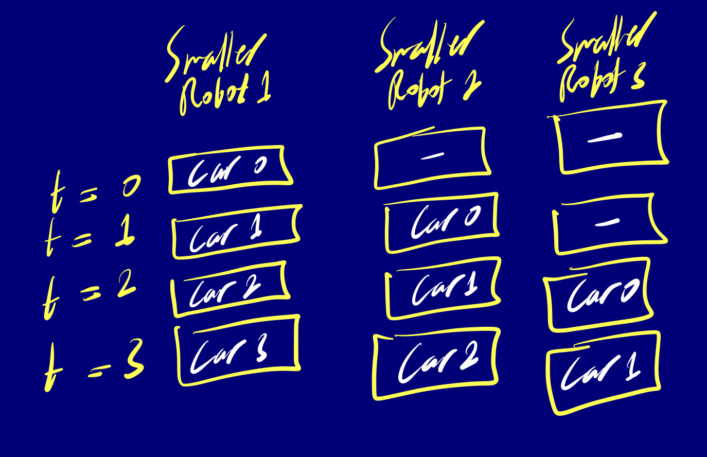
This way the factory has ramped up: the pipeline is now full!
Pipelining a MIPS Processor
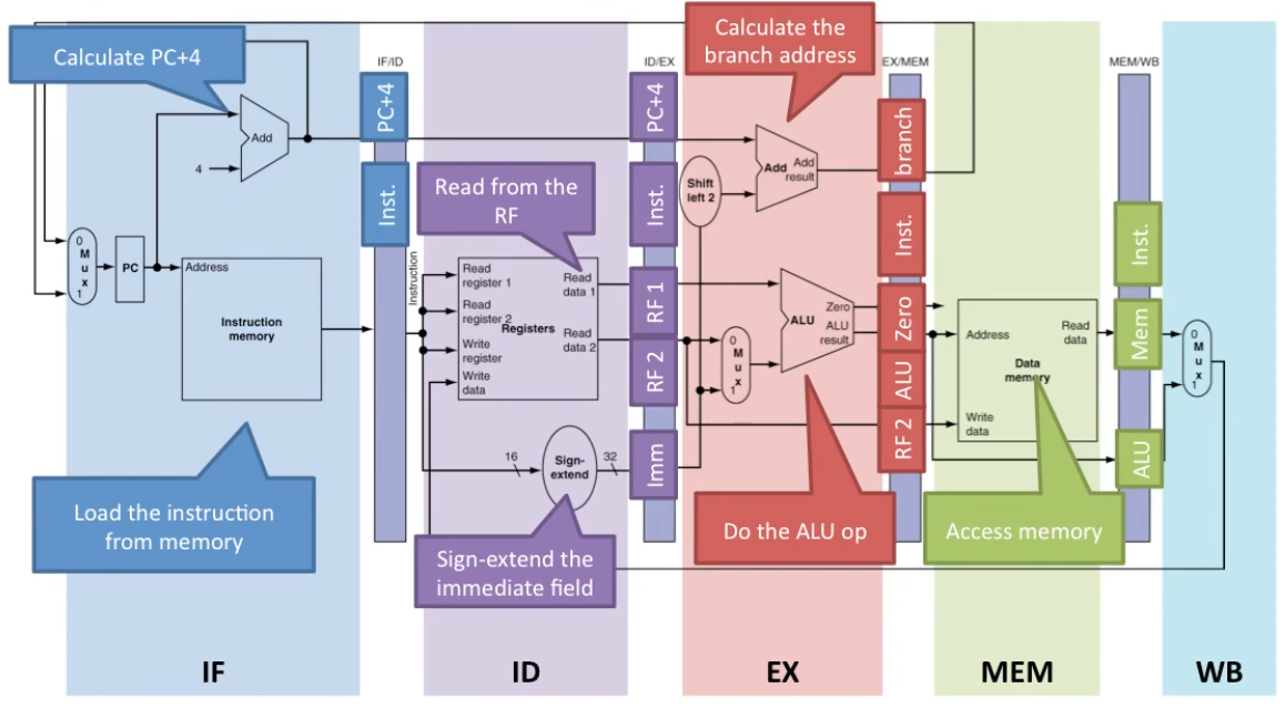
Pipelining a MIPS Processor involves optimizing the execution of instructions through a structured sequence of stages. Here’s a breakdown of the five key steps in pipelining:
-
Fetch: In this initial stage, the processor pulls the instruction from RAM into its pipeline.
-
Decode: Next, the type of the instruction is determined, and relevant details like register indices and immediate values are extracted.
-
Execute: If necessary, the arithmetic operation associated with the instruction is performed during this stage.
-
Memory: If required, the processor reads from or writes to RAM, contributing to the completion of the instruction.
-
Writeback: In the final stage, the processor updates a register with the result of an arithmetic operation or a RAM read, if applicable.
By placing each of these steps into its own hardware stage, the processor achieves an increased number of finished instructions per time unit. This pipeline concept, akin to the car production analogy, enhances efficiency. The processor’s clock frequency indicates the rate at which its pipeline successfully completes instructions. I found this great pipeline walkthrough video which explains far better than I could in writing.
Conclusion
This blog post set the groundwork. Everything I talked about is super important for what’s coming next. In the next post, I will focus on the detailed design and hands-on construction of the 32-bit MIPS ALU.
Last Edited: December 29, 2023