In the motivation post, I basically laid down the groundwork. I talked about all the basic stuff and essential concepts that we need to know before diving into the design. It was a good refresher for me as well.
Now, let’s shift gears a bit. I want to make one thing clear before doing anything: my Final Year Project isn’t about building a MIPS processor from scratch. Instead, it’s all about crafting an ALU (Arithmetic Logic Unit) that can meet the demands of our hardware realization of the MIPS CPU datapath. In order to check if our designed ALU works fine, I’ll need to also design a basic MIPS architecture to ensure the ALU fits into it seamlessly. However, I’ll be upfront: my primary focus will be on the ALU itself. That said, understanding how the ALU integrates into the MIPS architecture is essential. It’s like fitting a piece into a puzzle: each component needs to align perfectly for the whole system to function smoothly. So, while I won’t delve too deeply into the intricacies of MIPS, I’ll provide enough context to illustrate how our ALU fits into the bigger picture.
- Arithmetic Logic Unit
- FPGA
- Describing the Single Cycle MIPS CPU
- 32-bit MIPS Assembler [C++]
- Simulation on Cyclone V SoC Development Kit
- Source Code
Arithmetic Logic Unit
At its core, the ALU is a combinational circuit embedded within a computer’s central processing unit (CPU) that executes arithmetic and bitwise functions on integer binary variables. In contrast, a floating-point unit (FPU) handles floating-point values.
From the ALU’s point of view, a floating-point number is a series of random bits. Since floating point numbers are base two numbers with a mantissa and an exponent, you can always perform floating point operations using the ALU, but it’s slower than using a dedicated hardware FPU. You don’t always need a dedicated FPU. For example, GCC (GNU Compiler Collection) includes a software emulation layer for floating-point operations. This layer enables processors without FPU hardware to execute floating-point calculations using software routines. However, software emulation tends to be slower than hardware-based processing.
ALU Operations
In designing my ALU, I aim to support 9 fundamental operations (Addition, Subtraction, AND, OR, XOR, NAND, NOR, Shift Left Logical, and Shift Right Logical) in a combinational circuit that calculates a 32-bit output based on two 32-bit inputs and a 4-bit input specifying the ALU operation to perform. The ALU also computes three flag bits (Zero, Carry, and Overflow).
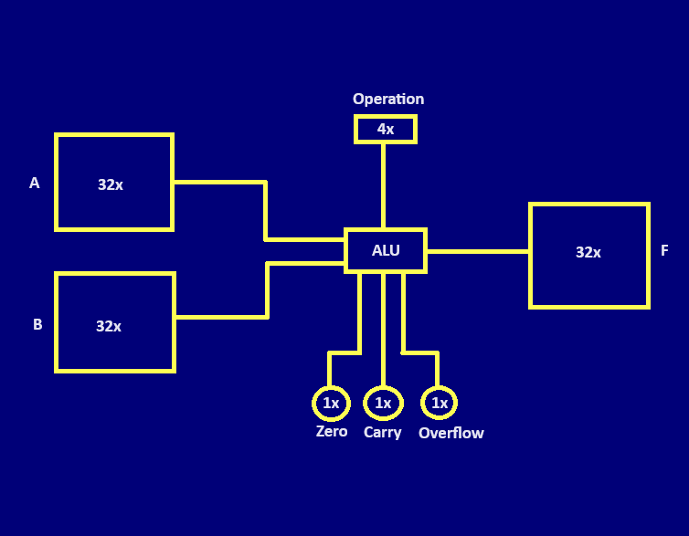
Now this is just an interface for the ALU: what goes in, what comes out. It also shows the ALU as an abstraction: you can’t see how it works, but you do know what it does.
Flag Bits
The three status outputs as well as the main result represent an answer to these questions: is the result zero, was there a carry, and did the operation result in an overflow?
Just a reminder on the difference between a carry and an overflow:
- Carry: Marks an outputted carry in the most-significant bit (MSB) due to limited bits.
- Overflow: Sign of output differs from inputs, signaling a change in magnitude (e.g., sum of two positives resulting in a negative).
Design Circuit
While the ultimate goal of my FYP typically involves using VHDL for practical integration into a larger system (MIPS), my focus here is on gaining a deep understanding of the inner workings of the ALU. By designing it in Logisim (A simulation environment for logic devices), we can grasp the fundamental concepts and operations that govern its functionality. This hands-on approach allows us to visualize and manipulate the digital circuitry. So, while the journey begins with a Logisim implementation for educational purposes, it sets the stage for a more practical application of VHDL later.
Starting with a 1-Bit ALU enables a systematic understanding and testing of operations before scaling up.
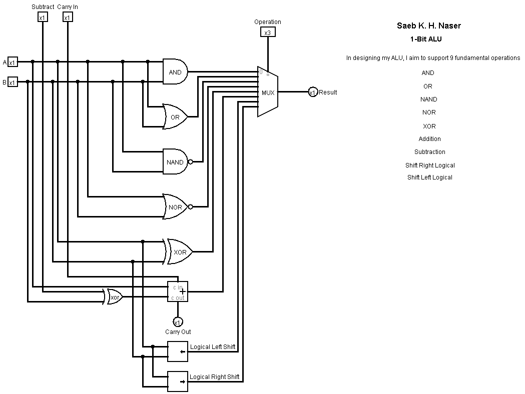
I’ve got gates lined up for all basic operations like AND, OR, NAND, NOR and XOR. Each gate takes the same 1-Bit inputs A and B. Now, when it comes to addition and subtraction, I’ve brought in an adder, complete with its own carry out pin. But here’s where it gets interesting: for subtraction in two’s complement style, I’ve added an XOR gate and a special input pin “Subtract”. Whenever I need the ALU to perform subtraction, I just assert that pin and surely the carry-in pin that comes into play whenever subtraction is on the table.
Lastly, for the logical shifts, I’ve thrown bit shifters: one for the left and another for right shifts. And to control which operation I need the ALU to perform, I’ve got a multiplexer with a 3-bit selector input. With that, I can pick between the eight operations: AND (000), OR (001), NAND (010), NOR (011), XOR (100), addition/subtraction (101), logical left shift (110), and logical right shift (111).
Note:
The logical left and right shifts in the 1-Bit ALU won’t function properly when we cascade 32 units of them. But they’re still part of the setup for future tweaks in VHDL.
This is me playing with the 1-Bit ALU :)
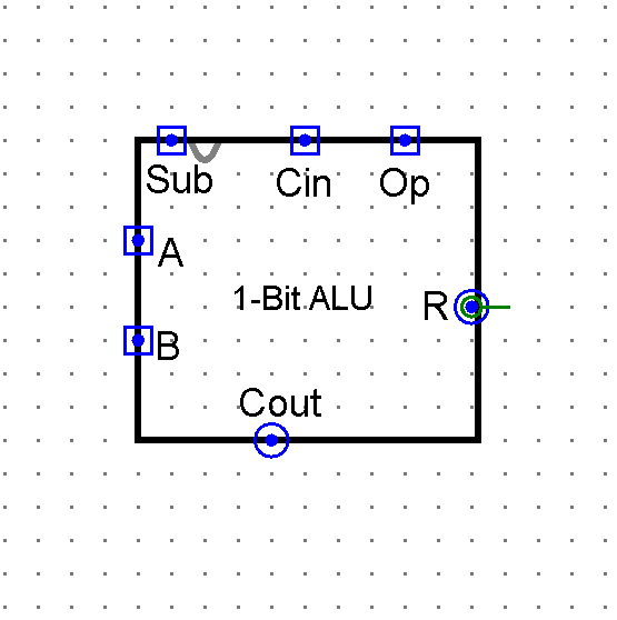
Instead of having the 1-Bit ALU viewed as a circuit layout, we can capture it in Logisim as an overall object by switching the mode from being the circuit’s Layout to the circuit’s Subcircuit Appearance.
Now, to get our fully operational 32-Bit ALU that performs our designated operations, we simply cascade 32 units of the 1-Bit ALU and ensure the correct connections between them.
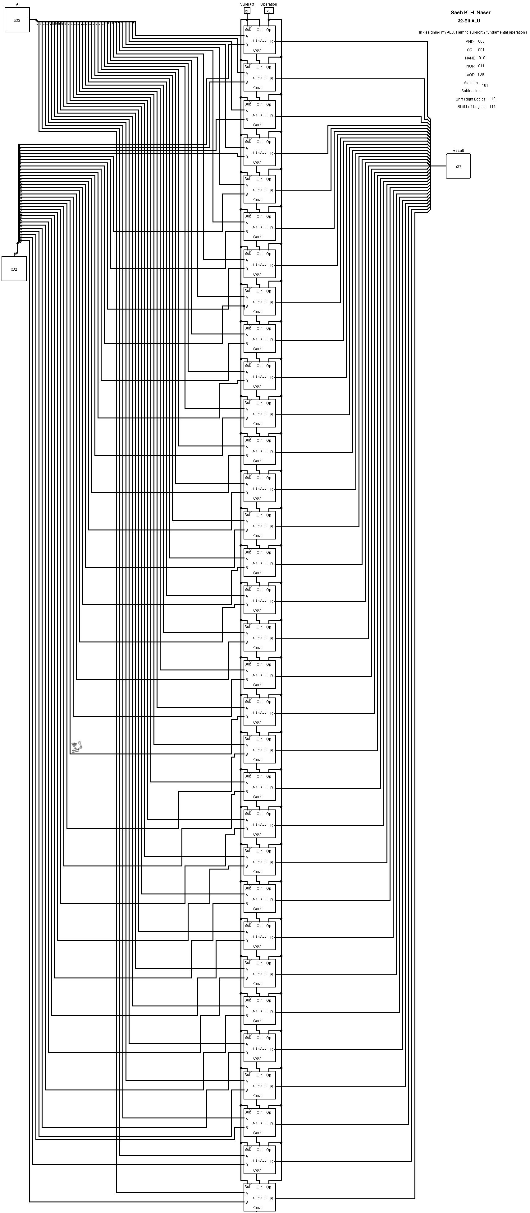
Much of the fun was in the design and learning, but the act of actually making the connections was a nightmare. Open the image in a new tab and zoom in to understand the circuit ansd try to spot Waldo ;)
We can also view our 32-Bit ALU as an Overall Object.
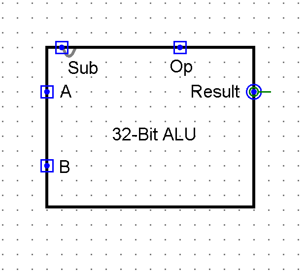
Now that things are starting to make sense, let’s move on to the next phase.
FPGA
I’ve always wanted to mess around with an FPGA, but many things have held me back. First off, they’re expensive (like, seriously expensive). Most FPGA development kits run over $100, and they often come with a bunch of features I don’t even need. And to top it off, some of them don’t even offer open-source toolchains.
Luckily, my supervisor came through with a Cyclone V SX SoC Development kit, which is more than great. Now our project is doable.
FPGA Versus Software Programming
Learning to code for an FPGA is quite the journey, very different from the typical CPU programming. When writing VHDL code for an FPGA, you’re essentially describing logic to build a CPU, whereas traditional programming runs directly on a CPU. It’s very crucial to recognize this distinction to avoid a lot of misconceptions.
The way that I started programming for the first time was by learning C, and code typically progresses linearly, executing one statement after another, from top to bottom (ignoring loops and such). However, in FPGA programming, everything operates concurrently (at the same time) as you’re defining circuits with multiple interconnected wires.
Adjusting to this parallel execution model is challenging, especially when I’m accustomed to CPU-based programming. In traditional programming, the order of statements matters, ensuring dependencies are properly addressed. Yet, in VHDL, the sequence of statements becomes irrelevant, as the entire design is evaluated as a whole.
I know I’m not an expert at this point, but I’m gradually understanding the HDL approach.
VHDL implementation
I’m very happy at this point, since we don’t need to make another connection. I was surprised to see that I was able to describe the previously implemented 32-Bit ALU in relatively few lines in VHDL. Something that took hours to connect and simulate in Logisim can be replaced with just a line or two.
In VHDL, you define the logical behavior of a circuit and trust the FPGA tools to synthesize your design into the appropriate gates on the FPGA. It’s very similar to writing a program in C and relying on the compiler to generate assembly code.
ALU
library IEEE;
use IEEE.std_logic_1164.all;
use IEEE.numeric_std.all;

entity ALU is
	GENERIC(n : integer := 32);
	port(
			-- Inputs
			operand_1 : in std_logic_vector(n - 1 downto 0);
			operand_2 : in std_logic_vector(n - 1 downto 0);
			ALU_control: in std_logic_vector(3 downto 0); -- 9 Operations

			-- Outputs
			result : out std_logic_vector(n - 1 downto 0);
			zero : out std_logic
		);
end ALU;

architecture Behavioral of ALU is
	signal temp : std_logic_vector(n - 1 downto 0);
	signal is_zero : std_logic;
begin
	-- ALU Operations
	with ALU_control select
		temp <= std_logic_vector(unsigned(operand_1) + unsigned(operand_2)) when "0000",
				std_logic_vector(unsigned(operand_1) - unsigned(operand_2)) when "0001",
				operand_1 AND operand_2 when "0010",
        		operand_1 OR operand_2 when "0011",
        		operand_1 NOR operand_2 when "0100",
        		operand_1 NAND operand_2 when "0101",
        		operand_1 XOR operand_2 when "0110",
				std_logic_vector(shift_left(unsigned(operand_1), to_integer(unsigned(operand_2)))) when "0111",
        		std_logic_vector(shift_right(unsigned(operand_1), to_integer(unsigned(operand_2)))) when "1000",
        		(others => '0') when others;

    -- Zero Detection
	process(temp)
	begin
		is_zero <= '1';
		for i in 0 to n - 1 loop
			if temp(i) /= '0' then
				is_zero <= '0';
				exit;
			end if;
		end loop;
	end process;

	zero <= is_zero;

	-- Output Result
	result <= temp;
end Behavioral;
Now, based on the given control signal, the ALU will perform arithmetic and logical operations on the two input operands.
To validate the functionality and ensure everything works fine, we can write a testbench. Testbenches are essential in VHDL Design. They serve as a simulation environment, providing input stimuli to the design under test (DUT) and evaluating its responses.
library IEEE;
use IEEE.std_logic_1164.all;
use IEEE.numeric_std.all;

entity Testbench_ALU is
end Testbench_ALU;

architecture Testbench of Testbench_ALU is
	-- Constants
	constant N_WIDTH : integer := 32;
	constant DELAY_PERIOD : time := 10 ns;

	-- Signals
	signal operand_1_tb : std_logic_vector(N_WIDTH - 1 downto 0);
	signal operand_2_tb : std_logic_vector(N_WIDTH - 1 downto 0);
	signal ALU_control_tb : std_logic_vector(3 downto 0);
	signal result_tb : std_logic_vector(N_WIDTH - 1 downto 0);
	signal zero_tb : std_logic;
begin
	-- Instantiate ALU
	ALU_inst : entity work.ALU
		generic map (n => N_WIDTH)
		port map (
				operand_1 => operand_1_tb,
				operand_2 => operand_2_tb,
				ALU_control => ALU_control_tb,
				result => result_tb,
				zero => zero_tb
			);

    -- Stimulus process
    stimulus : process
    begin
    	-- Test case for Addition
    	operand_1_tb <= "00000000000000000000000000000100";
        operand_2_tb <= "00000000000000000000000000000101";
        ALU_control_tb <= "0000";
        wait for DELAY_PERIOD;

         -- Test case for Subtraction
        operand_1_tb <= "00000000000000000000000000001000";
        operand_2_tb <= "00000000000000000000000000000100";
        ALU_control_tb <= "0001";
        wait for DELAY_PERIOD;

        -- Test case for AND
        operand_1_tb <= "00000000000000000000000000001111";
        operand_2_tb <= "00000000000000000000000000001100";
        ALU_control_tb <= "0010";
        wait for DELAY_PERIOD;

        -- Test case for OR
        operand_1_tb <= "00000000000000000000000000001010";
        operand_2_tb <= "00000000000000000000000000001100";
        ALU_control_tb <= "0011";
        wait for DELAY_PERIOD;

        -- Test case for NOR
        operand_1_tb <= "00000000000000000000000000001010";
        operand_2_tb <= "00000000000000000000000000001100";
        ALU_control_tb <= "0100";
        wait for DELAY_PERIOD;

        -- Test case for NAND
        operand_1_tb <= "00000000000000000000000000001010";
        operand_2_tb <= "00000000000000000000000000001100";
        ALU_control_tb <= "0101";
        wait for DELAY_PERIOD;

        -- Test case for XOR
        operand_1_tb <= "00000000000000000000000000001010";
        operand_2_tb <= "00000000000000000000000000001100";
        ALU_control_tb <= "0110";
        wait for DELAY_PERIOD;

         -- Test case for Shift Left Logical (SLL)
        operand_1_tb <= "00000000000000000000000000001010";
        operand_2_tb <= "00000000000000000000000000000010"; -- Shift by 2
        ALU_control_tb <= "0111";
        wait for DELAY_PERIOD;

        -- Test case for Shift Right Logical (SRL)
        operand_1_tb <= "00000000000000000000000000001010";
        operand_2_tb <= "00000000000000000000000000000010";
        ALU_control_tb <= "1000";
        wait for DELAY_PERIOD;

        -- Test case to check the zero flag
 		operand_1_tb <= "00000000000000000000000000001001";
 		operand_2_tb <= "00000000000000000000000000001001";
    	ALU_control_tb <= "0001"; -- Subtraction
		wait for DELAY_PERIOD;

		-- End simulation
        wait;
    end process stimulus;
end Testbench;
Simulation Waveform
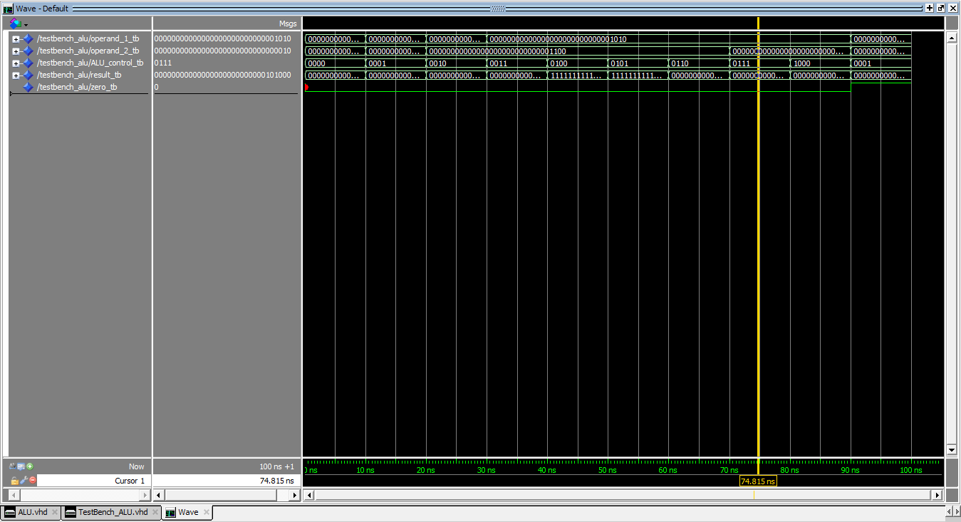
Note
I screenshotted the waveform from Intel ModelSim software, as I couldn’t find a better way to export it in higher quality. For better viewing, open it in a new tap. Feedback from experienced users on waveform exporting is welcome.
Describing the Single Cycle MIPS CPU
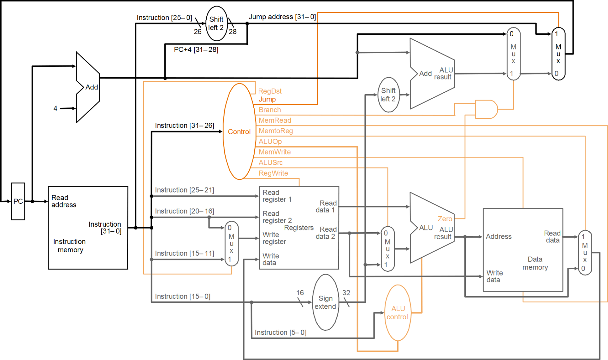
I talked about MIPS in details in my previous motivation blog post, including the key concepts of the architecture, the three instruction formats, and building a processor to execute MIPS instructions.
I’ll be following this diagram in my implementation.
Program Counter
The program counter synchronizes with the clock’s rising edge (transition from a low state 0 to a high state 1), always pointing to the next instruction. It includes an asynchronous reset for starting fresh. During normal operation, it follows the next instruction address, ensuring smooth execution and allowing jumps within the program.
library IEEE;
use IEEE.std_logic_1164.all;
use IEEE.numeric_std.all;

entity ProgramCounter is
	GENERIC (n : integer := 32);
	port(
		  -- Inputs
	      CLK        : in  std_logic; -- Clock signal
	      reset_neg  : in  std_logic;
	      next_address    : in  std_logic_vector(n - 1 downto 0);

	      -- Output
	      current_address : out std_logic_vector(n - 1 downto 0)
		);
end ProgramCounter;

architecture Behavioral of ProgramCounter is
begin
  process(CLK)
  begin
    if reset_neg = '0' then
      current_address <= (others => '0'); -- Clear address on reset
    elsif rising_edge(CLK) then
      current_address <= next_address;
    end if;
  end process;
end Behavioral;
Note
Asynchronous signals act right away without waiting for a clock, like an instant reset. Synchronous signals sync up with a clock’s rhythm, like a program counter updating on every tick.
Adder
The Adder adds two input operands together. It’ll be used in several places, like calculating the next PC value and in the ALU for arithmetic operations.
library IEEE;
use IEEE.std_logic_1164.all;
use IEEE.numeric_std.all;

entity Adder is
  GENERIC(n : integer := 32);
  port(
		-- Inputs
        operand_1 : in  std_logic_vector(n - 1 downto 0);
        operand_2 : in  std_logic_vector(n - 1 downto 0);

        -- Output
        result    : out std_logic_vector(n - 1 downto 0)
	   );
end Adder;

architecture Behavioral of Adder is
begin
  result <= std_logic_vector(unsigned(operand_1) + unsigned(operand_2));
end Behavioral;
Instruction Memory
The instruction memory stores the program instructions and provides them based on the given memory address.
library IEEE;
use IEEE.std_logic_1164.all;
use IEEE.numeric_std.all;

entity InstructionMemory is
  port(
		-- Input
        register_addr : in  std_logic_vector(31 downto 0);

        -- Output
        instruction   : out std_logic_vector(31 downto 0)
	   );
end InstructionMemory;

architecture Behavioral of InstructionMemory is
	type reg is array (0 to 1500) of std_logic_vector(7 downto 0);
		signal instr_memory: reg := (
			-- addi $R1,$R0,30
			0 => "00100000",
			1 => "00000001",
			2 => "00000000",
			3 => "00011110",

			-- sw $R1,0($R0)
			4 => "10101100",
			5 => "00000001",
			6 => "00000000",
			7 => "00000000",

			-- lw $R3,0($R0)
			8 => "10001100",
			9 => "00000011",
			10 => "00000000",
			11 => "00000000",

			-- srl $R7,$R3,1
			12 => "00000000",
			13 => "01100000",
			14 => "00111000",
			15 => "01000010",

			-- sll $R8,$R7,1
			16 => "00000000",
			17 => "11100000",
			18 => "01000000",
			19 => "01000000",

			-- addi $R2,$R0,27
			20 => "00100000",
			21 => "00000010",
			22 => "00000000",
			23 => "00011011",

			-- addi $R2,$R2,1
			24 => "00100000",
			25 => "01000010",
			26 => "00000000",
			27 => "00000001",

			-- sw $R2,1($R0)
			28 => "10101100",
			29 => "00000010",
			30 => "00000000",
			31 => "00000001",

			-- sub $R3,$R1,$R2
			32 => "00000000",
			33 => "00100010",
			34 => "00011000",
			35 => "00100010",

			-- beq $R1,$R2,1
			36 => "00010000",
			37 => "00100010",
			38 => "00000000",
			39 => "00000001",

			-- j 6
			40 => "00001000",
			41 => "00000000",
			42 => "00000000",
			43 => "00000110",

			-- sw $R2,3($R0)
			44 => "10101100",
			45 => "00000010",
			46 => "00000000",
			47 => "00000011",

			-- lw $R10,3($R0)
			48 => "10001100",
			49 => "00001010",
			50 => "00000000",
			51 => "00000011",

			others => "00000000"
		);
begin
  -- Concatenating four successive bytes to form a 32-bit instruction
  instruction <= instr_memory(to_integer(unsigned(register_addr)))     &
                 instr_memory(to_integer(unsigned(register_addr) + 1)) &
                 instr_memory(to_integer(unsigned(register_addr) + 2)) &
                 instr_memory(to_integer(unsigned(register_addr) + 3));
end Behavioral;
This instruction memory is byte-addressable, meaning that each address points to an individual byte of data. Each MIPS instruction is 32 bits long, equivalent to 4 bytes. To accommodate this, instructions are stored across four consecutive memory addresses. For instance, if an instruction starts at address 0, it will occupy the bytes at addresses 0, 1, 2, and 3.
To simplify it, the instruction memory will retrieve a full instruction by doing these steps:
- A 32-bit address is sent to the instruction memory.
- The memory will fetch four successive bytes starting from this address.
- These bytes are then concatenated in sequences to reconstruct the full 32-bit instruction.
The instruction memory contains a test program, but you can define your own program instructions by checking the 32-bit MIPS Assembler .
Multiplexer
The multiplexer is a data selector, it selects one of two inputs signals based on a control signal.
library IEEE;
use IEEE.std_logic_1164.all;
use IEEE.numeric_std.all;

entity Mux is
  GENERIC(n : integer := 32);
  port(
		-- Inputs
        input_1    : in std_logic_vector(n - 1 downto 0);
        input_2    : in std_logic_vector(n - 1 downto 0);
        mux_select : in std_logic; -- Control signal for selecting input

        -- Output
        output     : out std_logic_vector(n - 1 downto 0)
	   );
end Mux;

architecture Behavioral of Mux is
begin
with mux_select select
  output <= input_1 when '0', input_2 when others;
end Behavioral;
Registers
Registers store data and operands temporarily during program execution.
library IEEE;
use IEEE.std_logic_1164.all;
use IEEE.numeric_std.all;

entity Registers is
  GENERIC(n : integer := 32);
  port(
		-- Inputs
        CLK          : in std_logic;
        reset_neg    : in std_logic;
        address_in_1 : in std_logic_vector(4 downto 0);
        address_in_2 : in std_logic_vector(4 downto 0);
        address_out  : in std_logic_vector(4 downto 0);

        write_data   : in std_logic_vector(n - 1 downto 0);
        RegWrite     : in std_logic;  -- Control signal

        -- Outputs
        register_1   : out std_logic_vector(n - 1 downto 0);
        register_2   : out std_logic_vector(n - 1 downto 0)
	   );
end Registers;

architecture Behavioral of Registers is
  type registers_type is array (0 to 31) of std_logic_vector(n - 1 downto 0);
  signal reg : registers_type := ((others => (others => '0')));
begin
  -- Process for handling reset and write operations
  process(CLK)
  begin
    if reset_neg = '0' then
      reg(to_integer(unsigned(address_out))) <= (others => '0');
      else if rising_edge(CLK) and RegWrite = '1' then
        reg(to_integer(unsigned(address_out))) <= write_data;
      end if;
    end if;
  end process;

  register_1 <= reg(to_integer(unsigned(address_in_1)));  -- Read in address 1
  register_2 <= reg(to_integer(unsigned(address_in_2)));  -- Read in address 2
end Behavioral;
The main operations are performed on changes to the CLK signal. When the reset_neg signal is low 0, indicating an active-low reset condition, it sets the specified register (indicated by address_out) to zero. This is a focused reset, affecting only one register.
On the rising edge of the clock (CLK), if the RegWrite signal is high 1, the data from write_data is written into the register specified by address_out. This operation allows updating of register contents during normal operation.
The module continuously assigns values from the register file to the outputs register_1 and register_2. These assignments use address_in_1 and address_in_2 to select which registers’ contents are read, making these outputs always reflect the current contents of the specified registers.
Sign Extend
Sign Extend module will extend a 16-bit input value to a 32-bit signed value by sign-extending the MSB.
library IEEE;
use IEEE.std_logic_1164.all;
use IEEE.numeric_std.all;

entity SignExtend is
  port(
		-- Input
        input  : in std_logic_vector(15 downto 0); -- 16-bit

        -- Output
        output : out std_logic_vector(31 downto 0) -- 32-bit sign-extended
	   );
end SignExtend;

architecture Behavioral of SignExtend is
begin
 -- Based on the MSB of the input
 output <= "0000000000000000" & input when (input(15) = '0') else
           "1111111111111111" & input;
end Behavioral;
If the 16-bit input has an MSB of 0 (positive), it prepends 16 zero bits to it, maintaining the value as positive in a 32-bit signed format. On the other hand, if the MSB is 1 (negative), it prepends 16 one bits to it, effectively extending the sign and preserving the negative value in two’s complement form.
Shift Left 2
Shift Left 2 module shifts the input value to the left by two positions, effectively multiplying it by 4. If you read the motivation post, you would rememebr that when I talked about bit shifting, I mentioned that left shifting multiplies the number by 2 for each shift, while right shifting divides it by 2.
library IEEE;
use IEEE.std_logic_1164.all;
use IEEE.numeric_std.all;

entity ShiftLeft2 is
  port(
		-- Input
        input  : in std_logic_vector(31 downto 0);

        -- Output
        output : out std_logic_vector(31 downto 0)
	   );
end ShiftLeft2;

architecture Behavioral of ShiftLeft2 is
begin
  output <= std_logic_vector(unsigned(input) sll 2);
end Behavioral;
Data Memory
The data memory stores and retrieves data based on memory addresses. Used only for load and store instructions.
library IEEE;
use IEEE.std_logic_1164.all;
use IEEE.numeric_std.all;

entity DataMemory is
  GENERIC(n : integer := 32);
  port(
		-- Inputs
        CLK            : in std_logic;
        reset_neg      : in std_logic;
        memory_address : in std_logic_vector(n - 1 downto 0);
        MemWrite       : in std_logic;
        MemRead        : in std_logic;
        data_in        : in std_logic_vector(n - 1 downto 0);

        -- Output
        data_out       : out std_logic_vector(n - 1 downto 0)
       );
end DataMemory;

architecture Behavioral of DataMemory is
  type mem_type is array  (127 downto 0) of std_logic_vector(n - 1 downto 0); -- Holds 128 individual 32-bit values
  signal mem: mem_type;

begin
  process(CLK, reset_neg)
  begin
	 if reset_neg = '0' then
      mem <= (others => (others => '0'));
    elsif rising_edge(CLK) then
      if MemWrite = '1' then
        mem(to_integer(unsigned(memory_address))) <= data_in;
      end if;
    end if;
  end process;

  -- Continuous assignment for reading
  data_out <= (mem(to_integer(unsigned(memory_address)))) when MemRead = '1' else (others => '0');
end Behavioral;
Control Unit
The control unit has the most complicated behavior because that’s where most of the fun happens, it generates control signals for various components within the process based on the input instruction and other control signals.
library IEEE;
use IEEE.std_logic_1164.all;

entity ControlUnit is
  port(
		-- Inputs
        instruction : in std_logic_vector(31 downto 0);
        ZeroCarry   : in std_logic;

        -- Outputs (Control Signals)
        RegDst      : out std_logic;
        Jump        : out std_logic;
        Branch      : out std_logic;
        MemRead     : out std_logic;
        MemToReg    : out std_logic;
        ALUOp       : out std_logic_vector (3 downto 0);
        MemWrite    : out std_logic;
        ALUSrc      : out std_logic;
        RegWrite    : out std_logic
       );
end ControlUnit;

architecture Behavioral of ControlUnit is
  signal data : std_logic_vector(11 downto 0);  -- To set the control signals
begin
  -- According to the standard MIPS32 instruction reference
  -- R-type: Addition
  data <= "100000000001" when (instruction(31 downto 26) = "000000" and
                               instruction(10 downto 0)  = "00000100000") else
  -- R-type: Subtraction
  "100000001001" when (instruction(31 downto 26) = "000000" and
                       instruction(10 downto 0)  = "00000100010") else
  -- R-type: AND
  "100000010001" when (instruction(31 downto 26) = "000000" and
                       instruction(10 downto 0)  = "00000100100") else
  -- R-type: OR
  "100000011001" when (instruction(31 downto 26) = "000000" and
                       instruction(10 downto 0)  = "00000100101") else
  -- R-type: NOR
  "100000100001" when (instruction(31 downto 26) = "000000" and
                       instruction(10 downto 0)  = "00000100111") else
  -- R-type: XOR
  "100000110001" when (instruction(31 downto 26) = "000000" and
                       instruction(5 downto 0)   = "100110") else
  -- R-type: SLL (Shift Left Logical)
  "100000111011" when (instruction(31 downto 26) = "000000" and
                       instruction(5 downto 0)   = "000000") else
  -- R-type: SRL (Shift Right Logical)
  "100001000011" when (instruction(31 downto 26) = "000000" and
                       instruction(5 downto 0)   = "000010") else
  -- R-type: SLT (Set Less Than)
  "100001001001" when (instruction(31 downto 26) = "000000" and
                       instruction(10 downto 0)  = "00000101010") else
  -- I-type: Addition Immediate
  "000000000011" when instruction(31 downto 26) = "001000" else
  -- I-type: LW (Load Word)
  "000110000011" when instruction(31 downto 26) = "100011" else
  -- I-type: SW (Store Word)
  "000000000110" when instruction(31 downto 26) = "101011" else
  -- I-type: ANDI (AND Immediate)
  "000000010011" when instruction(31 downto 26) = "001100" else
  -- I-type: ORI (OR Immediate)
  "000000011011" when instruction(31 downto 26) = "001101" else
  -- I-type: BEQ (Branch on Equal)
  "001000001000" when instruction(31 downto 26) = "000100" else
  -- I-type: BNE (Branch on Not Equal)
  "001000110010" when instruction(31 downto 26) = "000101" else
  -- I-type: SLTI (Set Less Than Immediate)
  "000001001011" when instruction(31 downto 26) = "001010" else
  -- J-type: J (Jump)
  "010000000000" when instruction(31 downto 26) = "000010" else
  -- Otherwise
  (others =>'0');

  -- Set control signals based on the decoded data
  RegDst   <= data(11);
  Jump     <= data(10);
  -- AND port included considering the LSB of BEG and BNE
  Branch   <= data(9) AND (ZeroCarry XOR instruction(26));
  MemRead  <= data(8);
  MemToReg <= data(7);
  ALUOp    <= data(6 downto 3);
  MemWrite <= data(2);
  ALUSrc   <= data(1);
  RegWrite <= data(0);

end Behavioral;
The control unit decodes each instruction to generate control signals that direct the processor’s operation. It identities the operation type, such as arithmetic or branching, and activates the necessary components.
Note
Keep in mind that all MIPS instructions are encoded in binary, and this is what the 32-bit MIPS Assembler handles. All instruction have an opcode (op) that specifies the operation, which occupies the first 6 bits of the instruction. For R-type instructions, such as addition, subtraction, and logical operations, it is also necessary to examine the last 6 bits (function field) to determine the specific operation being performed.
Data Path
This module executes instructions by performing arithmetic and logical operations, accessing memory, and updating registers.
library IEEE;
use IEEE.std_logic_1164.all;

entity DataPath is
  GENERIC(n : integer := 32);
  port(
		-- Inputs
        CLK, reset_neg    : in std_logic;
        instruction       : in std_logic_vector(31 downto 0);

		-- Control Signals
        RegDst            : in std_logic;
        Jump              : in std_logic;
        Branch            : in std_logic;
        MemRead           : in std_logic;
        MemToReg          : in std_logic;
        ALUOp             : in std_logic_vector(3 downto 0);
        MemWrite          : in std_logic;
        ALUSrc            : in std_logic;
        RegWrite          : in std_logic;

		-- Outputs
        next_instruction  : out std_logic_vector(31 downto 0);
        ZeroCarry         : out std_logic
	   );
end DataPath;

architecture Behavioral of DataPath is

component ShiftLeft2 is
  port(
		-- Input
        input : in std_logic_vector(31 downto 0);

        -- Output
        output: out std_logic_vector(31 downto 0)
	   );
end component;

component SignExtend is
  port(
		-- Input
        input  : in std_logic_vector(15 downto 0);

        -- Output
        output : out std_logic_vector(31 downto 0)
	   );
end component;

component Mux is
  generic(n: integer);
  port(
		-- Inputs
        input_1    : in std_logic_vector(n - 1 downto 0);
        input_2    : in std_logic_vector(n - 1 downto 0);
        mux_select : in std_logic;

        -- Output
        output     : out std_logic_vector(n - 1 downto 0)
	   );
end component;

component DataMemory is
  port(
		-- Inputs
        CLK            : in std_logic;
        reset_neg      : in std_logic;
        memory_address : in std_logic_vector(n - 1 downto 0);
        MemWrite       : in std_logic;
        MemRead        : in std_logic;
        data_in        : in std_logic_vector(n - 1 downto 0);

        -- Output
        data_out       : out std_logic_vector(n - 1 downto 0)
	   );
end component;

component Registers is
  port(
		-- Inputs
        CLK          : in std_logic;
        reset_neg    : in std_logic;
        address_in_1 : in std_logic_vector(4 downto 0);
        address_in_2 : in std_logic_vector(4 downto 0);
        address_out  : in std_logic_vector(4 downto 0);

        write_data   : in std_logic_vector(n - 1 downto 0);
        RegWrite     : in std_logic;

        -- Outputs
        register_1   : out std_logic_vector(n - 1 downto 0);
        register_2   : out std_logic_vector(n - 1 downto 0)
	   );
end component;

component ProgramCounter is
port(
	  -- Inputs
      CLK        : in  std_logic;
      reset_neg  : in  std_logic;
      next_address      : in  std_logic_vector(31 downto 0);

      -- Output
      current_address     : out std_logic_vector(31 downto 0)
	 );
end component;

component Adder is
  port(
		-- Inputs
        operand_1 : in  std_logic_vector(n - 1 downto 0);
        operand_2 : in  std_logic_vector(n - 1 downto 0);

        -- Output
        result    : out std_logic_vector(n - 1 downto 0)
	   );
end component;

component ALU is
  port(
		-- Inputs
        operand_1   : in std_logic_vector(n - 1 downto 0);
        operand_2   : in std_logic_vector(n - 1 downto 0);
        ALU_control : in std_logic_vector(3 downto 0);  -- 9 Operations

        -- Outputs
        result      : out std_logic_vector(n - 1 downto 0);
        zero        : out std_logic
	   );
end component;

  constant PC_increment     : std_logic_vector(31 downto 0) := "00000000000000000000000000000100"; -- 4
  signal PC_out             : std_logic_vector(31 downto 0);
  signal MuxToWriteRegister : std_logic_vector(4 downto 0);
  signal SignExtendToSLL    : std_logic_vector(31 downto 0);
  signal SLLToAdder         : std_logic_vector(31 downto 0);
  signal ReadData1ToALU     : std_logic_vector(n-1 downto 0);
  signal ReadData2ToMux     : std_logic_vector(n-1 downto 0);
  signal MuxToALU           : std_logic_vector(n-1 downto 0);
  signal ALUToDataMemory    : std_logic_vector(n-1 downto 0);
  signal DataMemoryToMux    : std_logic_vector(n-1 downto 0);
  signal MuxToWriteData     : std_logic_vector(n-1 downto 0);
  signal AdderToMux         : std_logic_vector(31 downto 0);
  signal MuxToMux           : std_logic_vector(31 downto 0);
  signal MuxToPC            : std_logic_vector(31 downto 0);
  signal Adder1ToMux        : std_logic_vector(31 downto 0);
  signal SLLToMux           : std_logic_vector(31 downto 0);
  signal SLLOut             : std_logic_vector(31 downto 0);
  signal ShiftJump          : std_logic_vector(31 downto 0);

begin
  SLLToMux  <= Adder1ToMux(31 downto 28) & SLLOut(27 downto 0);
  ShiftJump <= "000000" & instruction(25 downto 0);

  Memory        : DataMemory     port map(CLK, reset_neg, ALUToDataMemory, MemWrite, MemRead, ReadData2ToMux, DataMemoryToMux);
  ALogicUnit    : ALU            port map(ReadData1ToALU, MuxToALU, ALUOp, ALUToDataMemory, ZeroCarry);

  MuxAlu        : Mux            generic map(32) port map(ReadData2ToMux, SignExtendToSLL, ALUSrc, MuxToALU);
  MuxReg        : Mux            generic map(5)  port map(instruction(20 downto 16), instruction(15 downto 11), RegDst, MuxToWriteRegister);
  MuxMem        : Mux            generic map(32) port map(ALUToDataMemory, DataMemoryToMux, MemToReg, MuxToWriteData);
  MuxBranch     : Mux            generic map(32) port map(Adder1ToMux, AdderToMux, Branch, MuxToMux);
  MuxJump       : Mux            generic map(32) port map(MuxToMux, SLLToMux, Jump, MuxToPC);
  AdderPC       : Adder          port map(PC_out, PC_increment, Adder1ToMux);
  AdderBranch   : Adder          port map(Adder1ToMux, SLLToAdder, AdderToMux);
  ShifterJump   : ShiftLeft2     port map(ShiftJump, SLLOut);
  ShifterBranch : ShiftLeft2     port map(SignExtendToSLL, SLLToAdder);
  ShiftExtend   : SignExtend     port map(instruction(15 downto 0), SignExtendToSLL);
  PC            : ProgramCounter port map(CLK, reset_neg, MuxToPC, PC_out);
  Registers1    : Registers      port map(CLK, reset_neg, instruction(25 downto 21), instruction(20 downto 16), MuxToWriteRegister, MuxToWriteData, RegWrite, ReadData1ToALU, ReadData2ToMux);

  next_instruction <= PC_out;
end Behavioral;
This data path ties together various components like ALU, PC, Registers, Memory, and Multiplexers to handle instruction fetching, decoding, execution, and the writing back of results. It represents the entire interface of the CPU.
32-bit MIPS Assembler
As previously discussed during the implementation of the instruction memory, designed to store program instructions, I integrated a test program. However, I want to provide a way to define custom programs using MIPS Assembly and simply passing them to a MIPS Assembler, which encodes the assembly instruction into machine code. Afterwards, you can load the encoded instructions into the instruction memory.
MIPSAssembler.h
#pragma once

#include <iostream>
#include <string>
#include <fstream>
#include <sstream>
#include <vector>
#include <unordered_map>
#include <algorithm>

const int NUMBIT = 16;

void Registers(std::string& reg);
void DecToBin(std::vector<int>& bin, int dec, int n);
int EncodeInstructions(const std::string& inputFile, const std::string& outputFile);
MIPSAssembler.cpp
#include "MIPSAssembler.h"

void Registers(std::string& reg)
{
    static const std::unordered_map<std::string, std::string> reg_map =
    {
        {"$R0", "00000"},  {"$R1", "00001"},  {"$R2", "00010"},  {"$R3", "00011"},
        {"$R4", "00100"},  {"$R5", "00101"},  {"$R6", "00110"},  {"$R7", "00111"},
        {"$R8", "01000"},  {"$R9", "01001"},  {"$R10", "01010"}, {"$R11", "01011"},
        {"$R12", "01100"}, {"$R13", "01101"}, {"$R14", "01110"}, {"$R15", "01111"},
        {"$R16", "10000"}, {"$R17", "10001"}, {"$R18", "10010"}, {"$R19", "10011"},
        {"$R20", "10100"}, {"$R21", "10101"}, {"$R22", "10110"}, {"$R23", "10111"},
        {"$R24", "11000"}, {"$R25", "11001"}, {"$R26", "11010"}, {"$R27", "11011"},
        {"$R28", "11100"}, {"$R29", "11101"}, {"$R30", "11110"}, {"$R31", "11111"}
    };

    if (reg_map.find(reg) != reg_map.end())
    {
        reg = reg_map.at(reg);
    }
    else
    {
        std::cerr << "ERROR: register can be Ri, with i=0,1,...,31\n";
        exit(EXIT_FAILURE);
    }
}

void DecToBin(std::vector<int>& bin, int dec, int n)
{
    bin.resize(n);
    for (int i = 0; i < n; i++)
    {
        bin[i] = (dec % 2 == 0) ? 0 : 1;
        dec /= 2;
    }

    std::reverse(bin.begin(), bin.end());
}

int EncodeInstructions(const std::string& inputFile, const std::string& outputFile) {
    std::ifstream fpin(inputFile);
    if (!fpin) {
        std::cerr << "Error opening input file\n";
        return EXIT_FAILURE;
    }

    std::ofstream fpout(outputFile);
    if (!fpout) {
        std::cerr << "Error opening output file\n";
        return EXIT_FAILURE;
    }

    std::string line, code, rd, rs, rt;
    int dec, cnt = 0;
    std::vector<int> b(NUMBIT);

    while (fpin >> code) {
        if (!strcmp(code.c_str(), "add")) { // add $R1 $R2 $R3
            fpin >> rd >> rs >> rt;

            fpout << "-- add " << rd << "," << rs << "," << rt << "\n";

            Registers(rd);
            Registers(rs);
            Registers(rt);

            fpout << cnt++ << " => \"000000" << rs[0] << rs[1] << "\",\n"
                << cnt++ << " => \"" << rs[2] << rs[3] << rs[4] << rt << "\",\n"
                << cnt++ << " => \"" << rd << "000\",\n"
                << cnt++ << " => \"00100000\",\n\n";
        }
        else if (!strcmp(code.c_str(), "sub")) { // sub $R1 $R2 $R3
            fpin >> rd >> rs >> rt;

            fpout << "-- sub " << rd << "," << rs << "," << rt << "\n";

            Registers(rd);
            Registers(rs);
            Registers(rt);

            fpout << cnt++ << " => \"000000" << rs[0] << rs[1] << "\",\n"
                << cnt++ << " => \"" << rs[2] << rs[3] << rs[4] << rt << "\",\n"
                << cnt++ << " => \"" << rd << "000\",\n"
                << cnt++ << " => \"00100010\",\n\n";
        }
        else if (!strcmp(code.c_str(), "addi")) { // addi $R1 $R2 50
            fpin >> rt >> rs >> dec;

            fpout << "-- addi " << rt << "," << rs << "," << dec << "\n";

            Registers(rt);
            Registers(rs);
            DecToBin(b, dec, NUMBIT);

            fpout << cnt++ << " => \"001000" << rs[0] << rs[1] << "\",\n"
                << cnt++ << " => \"" << rs[2] << rs[3] << rs[4] << rt << "\",\n";

            for (int j = 0; j < 2; ++j) {
                fpout << cnt++ << " => \"";
                for (int i = j * NUMBIT / 2; i < (j + 1) * NUMBIT / 2; ++i) {
                    fpout << b[i];
                }
                fpout << "\",\n";
            }
            fpout << "\n";
        }
        else if (!strcmp(code.c_str(), "lw")) { // lw $R1 50 $R2
            fpin >> rt >> dec >> rs;

            fpout << "-- lw " << rt << "," << dec << "(" << rs << ")\n";

            Registers(rt);
            DecToBin(b, dec, NUMBIT);
            Registers(rs);

            fpout << cnt++ << " => \"100011" << rs[0] << rs[1] << "\",\n"
                << cnt++ << " => \"" << rs[2] << rs[3] << rs[4] << rt << "\",\n";

            for (int j = 0; j < 2; ++j) {
                fpout << cnt++ << " => \"";
                for (int i = j * NUMBIT / 2; i < (j + 1) * NUMBIT / 2; ++i) {
                    fpout << b[i];
                }
                fpout << "\",\n";
            }
            fpout << "\n";
        }
        else if (!strcmp(code.c_str(), "sw")) { // sw $R1 50 $R2
            fpin >> rt >> dec >> rs;

            fpout << "-- sw " << rt << "," << dec << "(" << rs << ")\n";

            Registers(rt);
            DecToBin(b, dec, NUMBIT);
            Registers(rs);

            fpout << cnt++ << " => \"101011" << rs[0] << rs[1] << "\",\n"
                << cnt++ << " => \"" << rs[2] << rs[3] << rs[4] << rt << "\",\n";

            for (int j = 0; j < 2; ++j) {
                fpout << cnt++ << " => \"";
                for (int i = j * NUMBIT / 2; i < (j + 1) * NUMBIT / 2; ++i) {
                    fpout << b[i];
                }
                fpout << "\",\n";
            }
            fpout << "\n";
        }
        else if (!strcmp(code.c_str(), "and")) { // and $R1 $R2 $R3
            fpin >> rd >> rs >> rt;

            fpout << "-- and " << rd << "," << rs << "," << rt << "\n";

            Registers(rd);
            Registers(rs);
            Registers(rt);

            fpout << cnt++ << " => \"000000" << rs[0] << rs[1] << "\",\n"
                << cnt++ << " => \"" << rs[2] << rs[3] << rs[4] << rt << "\",\n"
                << cnt++ << " => \"" << rd << "000\",\n"
                << cnt++ << " => \"00100100\",\n\n";
        }
        else if (!strcmp(code.c_str(), "or")) { // or $R1 $R2 $R3
            fpin >> rd >> rs >> rt;

            fpout << "-- or " << rd << "," << rs << "," << rt << "\n";

            Registers(rd);
            Registers(rs);
            Registers(rt);

            fpout << cnt++ << " => \"000000" << rs[0] << rs[1] << "\",\n"
                << cnt++ << " => \"" << rs[2] << rs[3] << rs[4] << rt << "\",\n"
                << cnt++ << " => \"" << rd << "000\",\n"
                << cnt++ << " => \"00100101\",\n\n";
        }
        else if (!strcmp(code.c_str(), "nor")) { // nor $R1 $R2 $R3
            fpin >> rd >> rs >> rt;

            fpout << "-- nor " << rd << "," << rs << "," << rt << "\n";

            Registers(rd);
            Registers(rs);
            Registers(rt);

            fpout << cnt++ << " => \"000000" << rs[0] << rs[1] << "\",\n"
                << cnt++ << " => \"" << rs[2] << rs[3] << rs[4] << rt << "\",\n"
                << cnt++ << " => \"" << rd << "000\",\n"
                << cnt++ << " => \"00100111\",\n\n";
        }
        else if (!strcmp(code.c_str(), "andi")) { // andi $R1 $R2 50
            fpin >> rt >> rs >> dec;

            fpout << "-- andi " << rt << "," << rs << "," << dec << "\n";

            Registers(rt);
            Registers(rs);
            DecToBin(b, dec, NUMBIT);

            fpout << cnt++ << " => \"001100" << rs[0] << rs[1] << "\",\n"
                << cnt++ << " => \"" << rs[2] << rs[3] << rs[4] << rt << "\",\n";

            for (int j = 0; j < 2; ++j) {
                fpout << cnt++ << " => \"";
                for (int i = j * NUMBIT / 2; i < (j + 1) * NUMBIT / 2; ++i) {
                    fpout << b[i];
                }
                fpout << "\",\n";
            }
            fpout << "\n";
        }
        else if (!strcmp(code.c_str(), "ori")) { // ori $R1 $R2 50
            fpin >> rt >> rs >> dec;

            fpout << "-- ori " << rt << "," << rs << "," << dec << "\n";

            Registers(rt);
            Registers(rs);
            DecToBin(b, dec, NUMBIT);

            fpout << cnt++ << " => \"001101" << rs[0] << rs[1] << "\",\n"
                << cnt++ << " => \"" << rs[2] << rs[3] << rs[4] << rt << "\",\n";

            for (int j = 0; j < 2; ++j) {
                fpout << cnt++ << " => \"";
                for (int i = j * NUMBIT / 2; i < (j + 1) * NUMBIT / 2; ++i) {
                    fpout << b[i];
                }
                fpout << "\",\n";
            }
            fpout << "\n";
        }
        else if (!strcmp(code.c_str(), "xor")) { // xor $R1 $R2 $R3
            fpin >> rd >> rs >> rt;

            fpout << "-- xor " << rd << "," << rs << "," << rt << "\n";

            Registers(rd);
            Registers(rs);
            Registers(rt);

            fpout << cnt++ << " => \"000000" << rs[0] << rs[1] << "\",\n"
                << cnt++ << " => \"" << rs[2] << rs[3] << rs[4] << rt << "\",\n"
                << cnt++ << " => \"" << rd << "000\",\n"
                << cnt++ << " => \"00100110\",\n\n";
        }
        else if (!strcmp(code.c_str(), "sll")) { // sll $R1 $R2 10
            fpin >> rd >> rt >> dec;

            fpout << "-- sll " << rd << "," << rt << "," << dec << "\n";

            Registers(rd);
            Registers(rt);
            DecToBin(b, dec, NUMBIT);

            fpout << cnt++ << " => \"000000" << rt[0] << rt[1] << "\",\n"
                << cnt++ << " => \"" << rt[2] << rt[3] << rt[4] << "00000\",\n"
                << cnt++ << " => \"" << rd << b[11] << b[12] << b[13] << "\",\n"
                << cnt++ << " => \"" << b[14] << b[15] << "000000\",\n\n";
        }
        else if (!strcmp(code.c_str(), "srl")) { // srl $R1 $R2 10
            fpin >> rd >> rt >> dec;

            fpout << "-- srl " << rd << "," << rt << "," << dec << "\n";

            Registers(rd);
            Registers(rt);
            DecToBin(b, dec, NUMBIT);

            fpout << cnt++ << " => \"000000" << rt[0] << rt[1] << "\",\n"
                << cnt++ << " => \"" << rt[2] << rt[3] << rt[4] << "00000\",\n"
                << cnt++ << " => \"" << rd << b[11] << b[12] << b[13] << "\",\n"
                << cnt++ << " => \"" << b[14] << b[15] << "000010\",\n\n";
        }
        else if (!strcmp(code.c_str(), "beq")) { // beq $R1 $R2 25
            fpin >> rs >> rt >> dec;

            fpout << "-- beq " << rs << "," << rt << "," << dec << "\n";

            Registers(rs);
            Registers(rt);
            DecToBin(b, dec, NUMBIT);

            fpout << cnt++ << " => \"000100" << rs[0] << rs[1] << "\",\n"
                << cnt++ << " => \"" << rs[2] << rs[3] << rs[4] << rt << "\",\n";

            for (int j = 0; j < 2; ++j) {
                fpout << cnt++ << " => \"";
                for (int i = j * NUMBIT / 2; i < (j + 1) * NUMBIT / 2; ++i) {
                    fpout << b[i];
                }
                fpout << "\",\n";
            }
            fpout << "\n";
        }
        else if (!strcmp(code.c_str(), "bne")) { // bne $R1 $R2 25
            fpin >> rs >> rt >> dec;

            fpout << "-- bne " << rs << "," << rt << "," << dec << "\n";

            Registers(rs);
            Registers(rt);
            DecToBin(b, dec, NUMBIT);

            fpout << cnt++ << " => \"000101" << rs[0] << rs[1] << "\",\n"
                << cnt++ << " => \"" << rs[2] << rs[3] << rs[4] << rt << "\",\n";

            for (int j = 0; j < 2; ++j) {
                fpout << cnt++ << " => \"";
                for (int i = j * NUMBIT / 2; i < (j + 1) * NUMBIT / 2; ++i) {
                    fpout << b[i];
                }
                fpout << "\",\n";
            }
            fpout << "\n";
        }
        else if (!strcmp(code.c_str(), "slt")) { // slt $R1 $R2 $R3
            fpin >> rd >> rs >> rt;

            fpout << "-- slt " << rd << "," << rs << "," << rt << "\n";

            Registers(rd);
            Registers(rs);
            Registers(rt);

            fpout << cnt++ << " => \"000000" << rs[0] << rs[1] << "\",\n"
                << cnt++ << " => \"" << rs[2] << rs[3] << rs[4] << rt << "\",\n"
                << cnt++ << " => \"" << rd << "000\",\n"
                << cnt++ << " => \"00101010\",\n\n";
        }
        else if (!strcmp(code.c_str(), "slti")) { // slti $R1 $R2 50
            fpin >> rt >> rs >> dec;

            fpout << "-- slti " << rt << "," << rs << "," << dec << "\n";

            Registers(rt);
            Registers(rs);
            DecToBin(b, dec, NUMBIT);

            fpout << cnt++ << " => \"001010" << rs[0] << rs[1] << "\",\n"
                << cnt++ << " => \"" << rs[2] << rs[3] << rs[4] << rt << "\",\n";

            for (int j = 0; j < 2; ++j) {
                fpout << cnt++ << " => \"";
                for (int i = j * NUMBIT / 2; i < (j + 1) * NUMBIT / 2; ++i) {
                    fpout << b[i];
                }
                fpout << "\",\n";
            }
            fpout << "\n";
        }
        else if (!strcmp(code.c_str(), "j")) { // j 2500
            fpin >> dec;

            fpout << "-- j " << dec << "\n";

            DecToBin(b, dec, 26);

            fpout << cnt++ << " => \"000010" << b[0] << b[1] << "\",\n";

            for (int j = 0; j < 3; ++j) {
                fpout << cnt++ << " => \"";
                for (int i = 2 + j * 8; i < 10 + j * 8; ++i) {
                    fpout << b[i];
                }
                fpout << "\",\n";
            }
            fpout << "\n";
        }
        else {
            std::cerr << "Instruction error!\n";
            return EXIT_FAILURE;
        }
    }

    return EXIT_SUCCESS;
}
Main.cpp
#include "MIPSAssembler.h"

int main(int argc, char* argv[])
{
	if (argc != 3)
	{
		std::cerr << "USAGE: MIPSAssembler <input_file.ext> <output_file_name.ext>\n";
		return EXIT_FAILURE;
	}

	return EncodeInstructions(argv[1], argv[2]);
}
The assembler operates by reading instructions from an input file, mapping register names to their binary representations using a lookup table, encoding each instruction into binary format, and writing the encoded instructions to an output file. The assembler is customized via command line arguments, which specify the input file containing the assembly instructions and the output file for the machine code, allowing to easily change input and output files without modifying the code.
For example, running ./MIPSAssembler input.asm output.bin processes the instructions in input.asm and writes the machine code to output.bin.
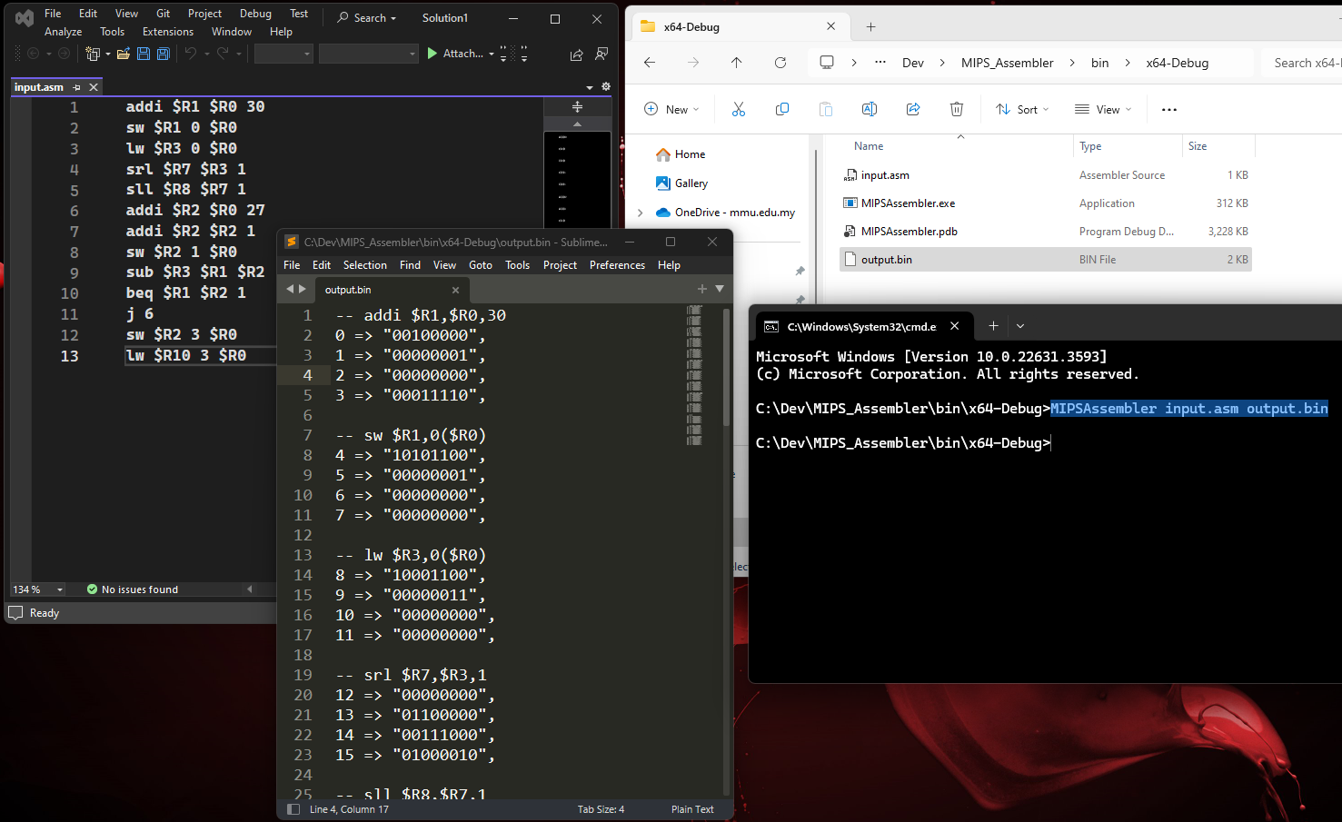
Now, we can easily write any program in MIPS Assembly and feed it to the instruction memory and test our processor.
Simulation on Cyclone V SoC Development Kit
In order to map the logical design to physical hardware on the Cyclone V SX FPGA, I need a top-level module. By assigning specific FPGA pins to inputs and outputs, such as the clock and reset signals, this module coordinates the flow of data and control across the processor’s components. It enables the synthesis and real-world testing of our MIPS architecture and, more importantly, our ALU.
library IEEE;
use IEEE.std_logic_1164.all;

entity TopLevel is
	GENERIC (n : integer := 32);
	port(
			-- Inputs
			CLK, reset_neg : in std_logic
		);
end TopLevel;

architecture Behavioral of TopLevel is

	component ControlUnit is
	port(
			-- Inputs
			instruction : in std_logic_vector(31 downto 0);
			ZeroCarry   : in std_logic;

			-- Outputs (Control Signals)
			RegDst      : out std_logic;
			Jump        : out std_logic;
			Branch      : out std_logic;
			MemRead     : out std_logic;
			MemToReg    : out std_logic;
			ALUOp       : out std_logic_vector (3 downto 0);  -- 9 Operations
			MemWrite    : out std_logic;
			ALUSrc      : out std_logic;
			RegWrite    : out std_logic
		 );
	end component;

	component DataPath is
	port(
			-- Inputs
			CLK, reset_neg    : in std_logic;
			instruction       : in std_logic_vector(31 downto 0);

			-- Control Signals
			RegDst            : in std_logic;
			Jump              : in std_logic;
			Branch            : in std_logic;
			MemRead           : in std_logic;
			MemToReg          : in std_logic;
			ALUOp             : in std_logic_vector(3 downto 0);
			MemWrite          : in std_logic;
			ALUSrc            : in std_logic;
			RegWrite          : in std_logic;

			-- Outputs
			next_instruction  : out std_logic_vector(31 downto 0);
			ZeroCarry         : out std_logic
		 );
	end component;

	component InstructionMemory is
	port(
			-- Input
			register_addr : in  std_logic_vector(31 downto 0);

			-- Output
			instruction   : out std_logic_vector(31 downto 0)
		 );
	end component;

	signal RegDst_TL, Jump_TL, Branch_TL, MemRead_TL, MemToReg_TL : std_logic;
	signal MemWrite_TL, ALUSrc_TL, RegWrite_TL , ZeroCarry_TL : std_logic;
	signal ALUOp_TL : std_logic_vector(3 downto 0);
	signal NextInstruction, instr : std_logic_vector(31 downto 0);
begin
	CU : ControlUnit  port map( instr,
	ZeroCarry_TL,
	RegDst_TL,
	Jump_TL,
	Branch_TL,
	MemRead_TL,
	MemToReg_TL,
	ALUOp_TL,
	MemWrite_TL,
	ALUSrc_TL,
	RegWrite_TL );

	DP : DataPath     port map( CLK,
	reset_neg,
	instr,
	RegDst_TL,
	Jump_TL,
	Branch_TL,
	MemRead_TL,
	MemToReg_TL,
	ALUOp_TL,
	MemWrite_TL,
	ALUSrc_TL,
	RegWrite_TL,
	NextInstruction,
	ZeroCarry_TL );

	I  : InstructionMemory  port map( NextInstruction, instr );
end Behavioral;
Before programming the FPGA with the VHDL design, I set it up for serial communication using PuTTY, to make sure everything was correctly configured.
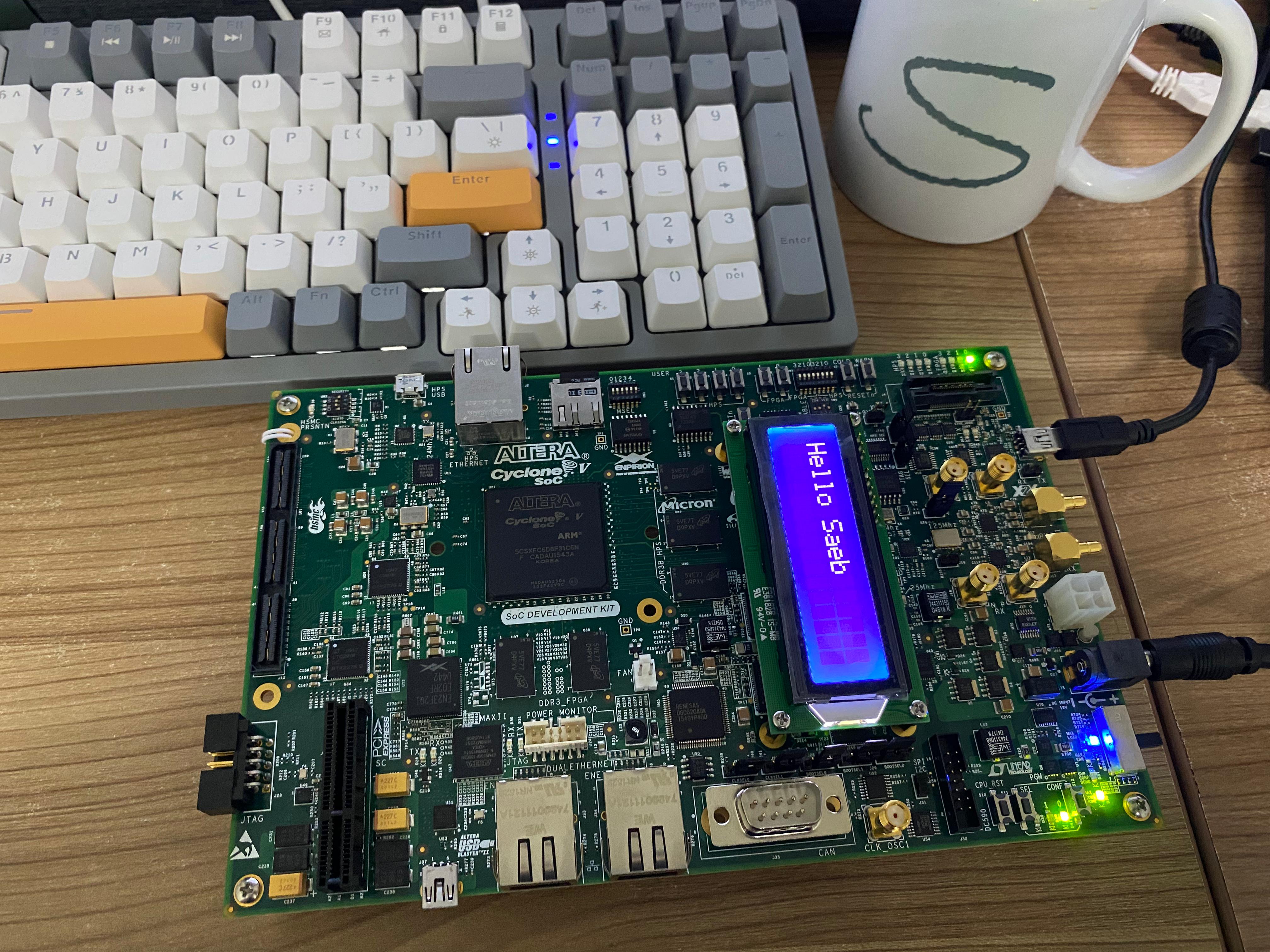
After thorough reading of the Cyclone V SoC Development Kit User Guide, I realized that the complexity and professional focus of the kit do not align with the tests I planned for this project. The kit’s lack of built-in user interaction components like 7-segment displays and push buttons makes it less suited for my immediate needs. While I could rig up an external circuit to add these features, why reinvent the wheel? I plan to discuss with my supervisor the possibility of switching to the DE1 board for this project, since I have some experience with it from my Digital Computer Design course. I think I’ll write a dedicated post about setting up a proper simulation environment.
Source Code
You can find all the code here.
Last Edited: May 17, 2024